10 Common DFM Mistakes That Cause PCB Production Failure
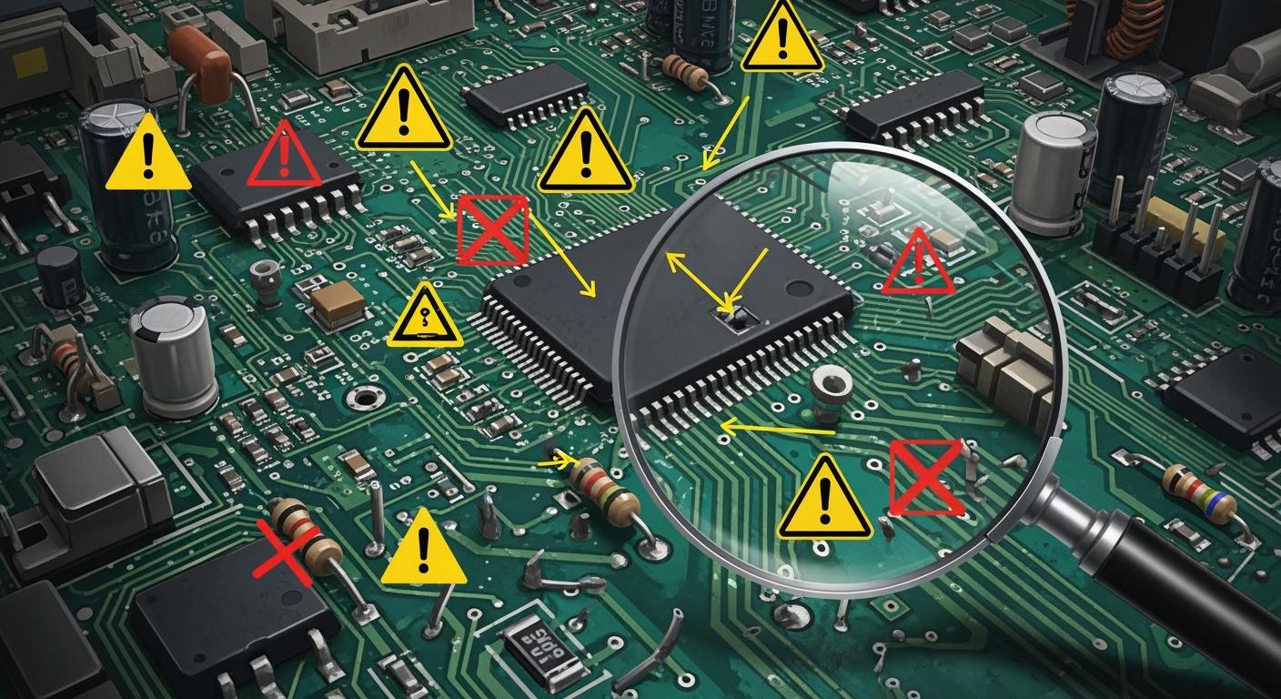
Most PCB production failures happen because of a few common DFM mistakes. If you think about DFM during design and layout, you help your PCB manufacturer avoid expensive problems and fewer defects. Early DFM review helps you find problems before production starts. When you focus on DFM, you make PCB manufacturing better. Look at these numbers:
Improvement Type | Percentage Improvement |
|---|---|
Yield Improvement | 5-20 percentage points |
Reduction in Defect Rates | Up to 30% |
You can stop mistakes in your board layout and avoid DFM mistakes by checking your design with your PCB manufacturer. This way helps you get good production and better results.
Key Takeaways
Pay attention to DFM when you design. This helps stop PCB problems and mistakes.
Look at trace width and spacing. This stops shorts and weak signals in your PCB.
Make sure pad sizes fit the component leads. This keeps solder joints strong.
Pick the right via specifications. This keeps signals clear and the PCB reliable.
Check your manufacturing files very carefully. This helps you avoid delays and expensive errors.
Trace Design DFM Mistakes in PCB
Trace Width and Spacing Issues
Trace width and spacing mistakes happen a lot in pcb manufacturing. These dfm mistakes can cause big problems when making pcbs. If traces are too thin or too close, you might get opens, shorts, or weak signals. You need to follow industry rules to stop these problems. The table below shows common mistakes and what they cause:
Violation Type | Impact on Manufacturing |
|---|---|
Inadequate Trace Width | Opens, shorts, or weak signals during use |
Tight Trace Spacing | Bridging during soldering, more defects |
Variations in Copper | Under-etching, unreliable pcb |
Trace Clearance Violations | Shorts, copper bridging, slivers during etching |
Improper Spacing | Arcing and signal problems |
Check your pcb design for these dfm mistakes before you send files to your manufacturer.
Overheating and Electrical Faults
Trace design mistakes can cause overheating and electrical faults in your pcb. High-power devices make heat if copper pours or vias are too small. This can cause thermal problems. High heat makes materials age faster and can cause big failures. Bad placement of high-power parts blocks airflow and makes hotspots. If power traces are not designed well, you can get voltage drops and overheating. These dfm mistakes make your pcb less reliable and can cause it to fail.
High-power devices make heat if copper pours or vias are too small.
High heat makes materials age faster and causes thermal runaway.
Not enough heat spreading makes hotspots that go over part limits.
Bad power trace design causes voltage drops and overheating.
How to Avoid Trace Problems
You can stop trace dfm mistakes by following industry rules. IPC-2221 tells you how wide traces should be to handle heat. IPC-9592 helps you set spacing for different voltages. UL 61010 gives clearance and creepage distances for safety. Keep traces apart to stop crosstalk and noise. Good spacing controls impedance and stops signal loss. Always check your pcb layout for these dfm mistakes before production.
Tip: Use your pcb manufacturer’s rules and run dfm checks to find trace mistakes early.
IPC-2221 tells trace width for heat management.
IPC-9592 sets spacing for power devices.
UL 61010 gives clearance for safety in industrial equipment.
Pad and Annular Ring Errors
Insufficient Pad Size
Pads need to be big enough for good soldering. If pads are too small, joints can be weak. Small pads make it hard for solder to flow. This can cause open circuits or bad connections. Always match pad size to the component leads. If you do not, you may have problems later.
Annular Ring Defects
Annular rings are copper rings around holes in your PCB. These rings help keep layers connected. If the ring is too small, you can get open circuits. Data shows that annular ring problems often cause PCB failures. The table below shows how these problems hurt production:
Evidence Description | Impact on PCB Production |
|---|---|
Not enough annular ring can break signal flow. | Causes open circuits. |
Annular ring breakouts happen when less than 2 mils. | Leads to production failures. |
Weak holes and bad desmear can change resistance. | Hurts long-term use and can cause failures. |
Annular rings help spot problems like bad plating. | Needed for quality checks. |
Always check your design for the right annular ring size. This helps you avoid expensive mistakes.
Pad Design Solutions
You can stop pad and annular ring problems by following some easy steps. Use the same pad shapes and sizes as your parts. Leave enough space between pads and the board edge. This stops damage when cutting or handling the board. Use the right footprints and place them well. This helps you avoid clearance and soldering problems.
Here are some quick tips for better pad design:
Use the same pad shapes to match leads and solder.
Do not put parts too close to the board edge to stop damage.
Make sure footprints and placement are correct to avoid problems.
Tip: Always check your pad and annular ring sizes with your PCB manufacturer’s rules. This helps you find mistakes before making the board.
Via Design for Manufacturing Issues
Incorrect Via Specs
You must watch via specs in your PCB layout. If vias are the wrong size, your board may not work. Small vias can make signals weak and cause bad connections. Big vias take up too much space and can hurt the board. Always use the right via size and spacing rules. Vias should be between 0.2mm and 0.3mm wide. Bigger vias are better for high-current paths. Keep vias at least two to three times their width away from important traces. This stops signal problems and makes building the board easier.
Tip: Talk to your manufacturer about via specs. Make sure they can meet your needs for annular ring size and drill-to-copper space.
Vias in Pads
If you put vias in pads without filling them, solder can move away during heating. This can make weak joints and bad connections. These problems can make your board fail over time. If vias are too close to surface mount pads, solder can move and make weak spots. For important boards, use filled and covered vias (VIPPO) to stop these problems. This helps solder stick better and keeps your board strong.
Reliable Via Design Tips
You can make your board better by following these via tips:
Pick the right via size for good signals.
Use more small vias together to lower inductance.
For fast designs, put vias under parts to cut resistance.
Blind or buried vias make signal paths shorter.
Keep at least 8 mil between drill and copper.
Make sure the annular ring is big enough to stop problems.
Through holes should have a 10:1 aspect ratio. Microvias should have a 0.75:1 ratio. Smaller ratios make boards easier to build and last longer.
Always check your design and run dfm checks before making your board. Good via design helps you avoid mistakes and makes your PCB work well. When you follow these rules, your board is easier to build and more reliable.
Solder Mask DFM Mistakes
Overlapping Pads
You need to watch for overlapping pads in your solder mask design. When pads overlap or sit too close to vias, you risk solder bridges and unstable connections. These mistakes can cause short circuits or make assembly harder. Solder mask dams help keep solder from running between pads. If you skip these dams, solder may follow copper paths and drop into holes, leading to electrical problems.
Issue Type | Result |
|---|---|
Overlapping pads and vias | Solder bridges, unstable connections |
Missing solder mask dams | Solder thieving, possible short circuits |
Always check your layout for overlapping pads and make sure you have enough solder mask dams between them.
Insufficient Openings
Solder mask openings must match the size and shape of your pads. If openings are too small, you may block solder from reaching the pad. If openings are too big, you expose too much copper and risk soldering defects. You should follow minimum web widths for different mask colors. For green and red, use at least 4 mil. For other colors, use 5 mil. IPC guidelines recommend a mask-to-pad clearance of 1.6 mil and a mask dam width of 4 mil.
Minimum web width for green and red: 4 mil
Minimum web width for other colors: 5 mil
Mask-to-pad clearance: 1.6 mil (IPC guideline)
Mask dam width: 4 mil
Check your solder mask openings before sending your files to the manufacturer.
Solder Mask Best Practices
You can avoid solder mask DFM mistakes by following these best practices:
Use a minimum solder mask dam size of 75um to ensure proper coverage. Designers often use 50um, but this is not enough.
Keep solder mask openings clear and sized to match your pads.
Follow IPC guidelines for clearance and dam width.
Make sure solder mask webs are wide enough for your chosen color.
Run DFM checks to spot mistakes early.
Tip: Always ask your PCB manufacturer for their solder mask rules. This helps you prevent soldering defects and keeps your board reliable.
Unbalanced Stack-Up in PCB Design
Stack-Up Problems
You need to pay close attention to your PCB stack-up. If you create an unbalanced stack-up, you risk many problems. When you place signal layers without a nearby ground plane, you increase electromagnetic interference (EMI). This happens because return paths become uneven. Asymmetrical layouts also cause bow, twist, and inconsistent thickness. These issues make your board hard to manufacture and assemble. You may see permanent warpage, which can lower assembly yield and weaken solder joints. Over time, thermal stress can make these problems worse.
Impact on Reliability
Stack-up imbalance does not just affect how your board looks. It can hurt your board’s reliability for its entire life. Warpage from an unbalanced stack-up can cause your board to fail after many heating and cooling cycles. Even if your board passes IPC standards at room temperature, it may not survive real-world use. Boards with more than 0.70% bow show a defect rate three to five times higher than boards with less than 0.40% bow. This can cost you thousands of dollars in lost yield and repairs.
Bow Measurement | Defect Rate Increase | Potential Savings |
|---|---|---|
> 0.70% | 3-5× higher | $120,000–200,000 |
< 0.40% | Baseline | N/A |
Stack-Up Design Tips
You can avoid stack-up problems by following these tips:
Tailor your stack-up for your signal speed, frequency, and power needs.
Balance copper on each layer to stop warping during lamination.
Place signal layers one dielectric away from ground planes to lower EMI.
Match trace width, spacing, and dielectric thickness to your target impedance.
Group signal layers by frequency to keep signals clean.
Pick the right dielectric material for good heat and signal control.
Add enough ground and power layers for better signal integrity.
Avoid putting signal layers next to each other to reduce EMI.
Tip: Always review your stack-up with your PCB manufacturer. This helps you catch problems before production starts.
Silkscreen and Marking Errors
Unclear Silkscreen Text
Your PCB needs clear silkscreen text. If you use small letters or put words too close, people cannot read them. Fuzzy or crowded text makes it hard for workers and machines to see what is written. When silkscreen is not clear, mistakes can happen during assembly and checking. You should pick bold, simple fonts and leave space between words. This way, everyone can see part numbers and polarity marks without guessing.
Assembly Confusion
If silkscreen markings are missing or hard to read, your assembly team can get confused. When parts are not labeled well, technicians may not know where each part goes. This can make them put parts in the wrong place or the wrong way. Sometimes, this causes products to not work right. It also slows down assembly because workers have to look for information longer.
Here is how silkscreen errors can make assembly confusing:
Evidence | Explanation |
|---|---|
Clear silkscreen markings help technicians during assembly. | If markings are wrong, parts can be put in the wrong place or turned the wrong way, which causes confusion. |
Good silkscreen designs make assembly faster and more accurate. | Without clear markings, it is hard to find where parts go, so mistakes happen and it takes more time. |
Easy-to-read markings show where parts should be placed. | If instructions are not clear, workers can make mistakes, which means more rework and higher costs. |
If silkscreen markings are not clear or missing, assemblers can get confused.
This confusion can cause SMT assembly problems, especially when checking or fixing boards by hand.
Silkscreen Guidelines
You can stop silkscreen DFM mistakes by following some easy rules:
Do not forget about silkscreen. Good markings save time and stop mistakes.
Do not use tiny letters or put words on top of each other. Big, clear letters help people and machines.
Make your silkscreen easy to read. This helps machines and makes training workers easier.
Keep silkscreen away from pads and vias so you do not get soldering problems.
Use standard symbols and clear marks to show polarity for all parts.
Tip: Always check your silkscreen layer before you send files to the manufacturer. Clear markings help everyone build your PCB right the first time.
Surface Finish Selection Mistakes
Incompatible Surface Finish
You have to pick the right surface finish for your PCB. Many people choose finishes that do not fit their board’s needs. If you pick the wrong finish, you might get solder problems or tarnish. Sometimes, people forget to say what finish they want in their notes. This can make the factory use the wrong coating. If your drawings and the way the board is made do not match, you can get bad layers. These mistakes can make your PCB not work well.
The wrong surface finish can cause solder problems or tarnish.
If you do not say the finish in your notes, you might get the wrong coating.
If your drawings and the factory do not match, you can get bad layers.
Tip: Always check your notes and drawings to make sure you say what finish you want.
Solderability Issues
Picking the wrong surface finish can make it hard to solder and hurt how long your board lasts. If the coating is not even, soldering will not work well. This can make your board not work right. If the finish gets rusty or tarnished, solder joints get weak. If solder does not stick well, you can get bridges, holes, or joints that are not finished. These problems make your board less reliable. If your finish does not match your parts, putting the board together can be hard. Your board might not work as it should.
Uneven coating makes soldering hard.
Rust and tarnish make solder joints weak.
Bad solder sticking causes bridges and holes.
If the finish does not fit the parts, assembly and use are hard.
Note: Good solder joints need the right surface finish.
Choosing the Right Finish
You need to pick a surface finish that matches what your PCB will do. Look at these points to help you choose:
Criteria | HASL Description | ENIG Description |
|---|---|---|
Desired shelf-life | Good for boards that do not need to last long or for test boards. | Great for boards that need to last a long time. |
Solderability | Works well for through-hole parts. | Very good for small, fine-pitch SMT parts. |
Dimensional tolerances | Okay for most uses. | Better for tight spaces because it is smooth. |
Environmental resilience | Fine for places that are not too tough. | Very strong in harsh places. |
Component compatibility | Best for through-hole parts. | Best for small, fine-pitch parts and wire bonding. |
Budgetary constraints | Cheaper if you want to save money. | Costs more but gives better results for tough jobs. |
Pick the finish that fits your board’s needs. HASL is good for simple and cheap boards. ENIG is better for boards that need to last and work well.
Tip: Ask your PCB maker which finish is best for your board. This helps you avoid mistakes and build a board you can trust.
Mechanical and Edge Clearance Issues
Overlooked Mechanical Constraints
You should think about mechanical constraints early in PCB design. If you forget these, your board can have problems later. Parts placed too close together make soldering hard. This can cause unwanted solder joints. Traces near parts can lead to electrical shorts. Not leaving enough space makes your board weak and hard to handle.
Here is a table showing common mechanical and edge clearance issues:
Issue Type | Description |
|---|---|
Clearance between Component and Component | Narrow spacing can hinder soldering and create unwanted joints. |
Features To-Copper Components | Traces too close to components may lead to electrical shorts. |
Component-to-Board Edge | Components near edges are more susceptible to damage. |
Solder Mask Incursion | Insufficient pad clearance under solder mask can compromise board reliability. |
Minimum Spacing for Tiny Components | 6 mil clearance is recommended. |
Minimum Spacing for Sensitive Devices | 39 mil clearance for sensitive devices like BGAs is advised. |
Distance from Board Edges | Components should be at least 50-75 mils away from edges. |
Solder Mask Clearance | 1.6 mils should be maintained between pad edges and solder mask to prevent incursion. |
Insufficient Edge Clearance
If you do not leave enough space between parts and the board edge, your PCB can get damaged. You should place most parts at least 0.1 inches (2.54 mm) from the edge. For bigger parts, use 0.2 inches (5 mm). Copper traces need at least 0.02 inches (0.5 mm) from the edge to stop shorts. Mounting holes and drilled holes also need enough space to avoid cracks.
Component Type | Minimum Clearance from Edge |
|---|---|
General Components | 0.1 inches (2.54 mm) |
Larger Components (e.g., connectors) | 0.2 inches (5 mm) |
Components near V-grooves | 0.05 inches (1.27 mm) |
Components near Breakout Tabs | 0.1 inches (2.54 mm) |
Copper Traces near Board Edge | 0.02 inches (0.5 mm) |
Mounting Holes | 0.125 inches (3.175 mm) |
Drilled Holes | 0.1 inches (2.54 mm) |
Routed Boards | 0.05 inches (1.27 mm) |
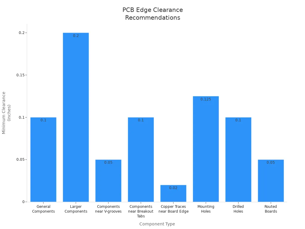
Note: Keeping enough space helps your board last longer and work better.
Mechanical Design Tips
You can stop mechanical and edge clearance mistakes by following these tips:
Place parts at least 0.1 inches (2.54 mm) from the board edge.
For big connectors or heavy parts, use 0.2 inches (5 mm) space.
Keep copper traces at least 0.02 inches (0.5 mm) from the edge.
Use 6 mil space for tiny parts and 39 mil for sensitive devices like BGAs.
Always check for enough space around mounting and drilled holes.
Review your design with your manufacturer’s rules before production.
Tip: Good planning keeps your PCB strong and reliable during assembly and use.
Incomplete Manufacturing Files
Missing or Wrong Data
You must send all files for every pcb project. If you forget a file or send wrong data, production cannot start. Common mistakes are missing drill files, wrong formats, or broken data. These mistakes cause delays in making the board. You may need to answer questions from your manufacturer. This can take three to five days. Errors in Gerber files or BOMs are very common pcb problems.
Issue Type | Impact on Production Delay |
|---|---|
Missing or Mismatched Drill Files | Production stops until you fix the files |
Solder Mask Openings Misalignment | You must explain, which causes delays |
Layer Naming Convention Issues | Causes confusion and stops production |
Undefined Layer Stack-up | Factory stops and asks for more details |
Production Delays and Errors
If you send incomplete files, you risk big delays. The factory cannot work without all the information. They may stop and ask you for missing details. This back-and-forth wastes time and money. You may get boards with mistakes if files are not clear. The pre-production phase is very important. If you do not check your files, you can cause delays and mistakes that are hard to fix later.
Incomplete files often cause big delays in production.
Errors in Gerber files and BOMs are common problems.
Fixing mistakes can take three to five days.
File Preparation Checklist
You can avoid these problems by using a checklist for pcb projects. Make sure you include all files your manufacturer needs. Here is a table of the most important files:
File name | What’s in it |
|---|---|
Gerber/ODB++ file | Top and bottom overlays, solder mask, silkscreen, drill drawing, tolerances |
Netlist | Name of the net, pin numbers, reference designators |
NC drill file | Drill sizes, hole types, and tolerances |
Component placement file | Position and direction of all SMDs |
PDFs | Assembly notes, fab notes, stack-up, impedance requirements |
BOM | List of all the parts to be assembled |
Tip: Always check your files before sending them to your manufacturer. Complete and correct files help you avoid delays and mistakes.
Component Placement DFM Mistakes
Overly Tight Placement
Every part needs enough space on your PCB. If parts are too close, assembly gets harder. Machines cannot place parts as accurately. Parts might touch each other and cause short circuits. It is hard to fix mistakes when parts are crowded. Tools cannot reach parts easily for repairs. Workers may miss errors because they cannot see parts well.
Tight spacing makes placement less accurate.
Parts can bump into each other more often.
Fixing mistakes is tough when parts are crowded.
Assembly Challenges
Bad placement causes problems during assembly. If you do not use the right footprints, parts may not line up. Missing pin marks make it hard to check parts. Overlapping areas can make parts bump into each other. If you skip test points, checking for errors is harder. Putting vias in pads without planning can make weak joints. Using many assembly methods on one board costs more and is more complex.
Here is a table showing common mistakes, their problems, and ways to avoid them:
Mistake | Problem | How to Avoid It |
|---|---|---|
Poor Component Footprint Definition/Courtyard Violations | Parts do not line up, missing pin marks, overlapping areas | Use the right footprints, check pad spacing and marks |
Ignoring Testability and Access for Inspection | Test pads are too small or hard to reach, more rework | Reserve test pads, ask test engineers for help early |
Placing Vias in Pads Without Proper Planning | Solder moves away, joints are weak | Use via-in-pad only when needed, fill vias the right way |
Overcomplicating the Board Layout | Costs more, assembly is harder | Put SMT parts on one side, use simple processes |
Placement Best Practices
You can stop most placement mistakes by following easy rules:
Leave space between parts for machines and tools.
Use the right footprints and clear marks for direction.
Make test pads easy to reach for checking.
Do not put vias in pads unless you fill them right.
Keep similar parts together and use one assembly method if you can.
Tip: Check your part placement with your manufacturer before finishing your design. This helps you find problems early and makes assembly easier.
You can prevent most PCB failures by avoiding these 10 common DFM mistakes. Careful checks and early talks with your manufacturer help you catch problems before they cost you time or money. Use the tips from this guide in your next design to improve your results.
Tip: Keep learning about DFM best practices. New rules and tools appear often. Stay updated to make your PCBs stronger and more reliable.
FAQ
What is the most common DFM mistake in PCB design?
Trace width and spacing errors happen a lot. These mistakes can make shorts or open circuits. Always check your design rules before you send files.
How can you avoid pad and annular ring problems?
Make sure pad sizes fit the component leads. Check annular ring sizes with your manufacturer’s rules. This helps stop open circuits and weak solder joints.
Why do incomplete manufacturing files delay PCB production?
Missing or wrong files stop the factory from working. Your manufacturer needs all the right data to build your board. Always use a checklist before you send your files.
What happens if you place components too close together?
Assembly gets harder.
Machines may not put parts in the right spot.
Repairs and checks take more time.
You can get short circuits and soldering issues.
How do DFM checks help you?
DFM checks find design mistakes early. You save time and money by fixing problems before making the board. Always run DFM checks with your manufacturer’s help.
See Also
Addressing Common Issues in SMT PCB Design Solutions
Understanding The Steps In The PCB Manufacturing Journey
Ten Effective Strategies To Reduce Custom PCB Production Costs
Achieving Excellence In Quality Control For PCB Production
Seven Essential Quality Control Measures For Heavy Copper PCBs