Guide to Stackup and Structure for 10 Layer HDI PCBs
An optimal 10 layer hdi pcb stackup utilizes stackup symmetry, advanced materials, and microvia technology to support high-speed, compact devices. When designing a 10 layer hdi pcb, you may encounter challenges such as routing complexity, impedance control, and thermal management. LT CIRCUIT offers specialized expertise in 10 layer hdi pcb solutions, ensuring you achieve reliable performance and robust stackup integrity.
Common Design Challenges in 10 Layer HDI PCB Stackups |
|---|
Routing complexity, impedance control, layer alignment, thermal management, manufacturing precision, cost, and EMI risk |
Key Takeaways
A symmetrical stackup in a 10 layer HDI PCB helps control impedance and improves manufacturability.
Proper layer allocation is crucial. Place ground planes next to signal layers to enhance signal integrity and reduce noise.
Using advanced materials like FR-4 or polyimide can significantly boost the performance and reliability of your 10 layer PCB.
10 Layer HDI PCB Stackup
Typical Layer Arrangement
When you design a 10 layer pcb stackup, you need to plan the arrangement of each layer carefully. The structure of a 10-layer pcb stackup supports high-speed signals, stable power delivery, and strong shielding against noise. Most hdi pcb stackup designs use a symmetrical layout to maintain consistent impedance and manufacturability. You often see signal layers sandwiched between ground and power planes. This arrangement helps you achieve better signal integrity and power integrity.
Here is a typical 10 layer pcb stackup used by leading manufacturers:
Layer Number | Layer Type | Function Description |
|---|---|---|
1 | Top Layer (Signal Layer) | Contains the topmost copper traces for signals between components and connectors. |
2 | Signal Layer 2 | Additional signal layer for more routing channels. |
3 | Ground Plane 1 | Provides a solid ground reference to reduce noise and EMI. |
4 | Power Plane 1 | Serves as a power distribution plane for components. |
5 | Internal Signal Layer 1 | Used for routing signals between components. |
6 | Internal Signal Layer 2 | Provides additional routing channels for signals. |
7 | Ground Plane 2 | Enhances shielding and reduces noise. |
8 | Power Plane 2 | Acts as an additional power distribution plane. |
9 | Signal Layer 3 | Provides more space for routing signals. |
10 | Bottom Layer (Signal Layer) | Contains copper traces for signals and interconnections. |
Tip: You should keep the stackup symmetrical. This helps you control impedance and makes the multilayer pcb stackup easier to manufacture.
Layer Functions
Each layer in your 10-layer pcb stackup has a specific role. You need to assign functions based on your pcb design requirements. The right allocation of signal, power, and ground layers improves hdi performance and reliability.
Signal Layers (Layers 1, 2, 5, 6, 9, 10):
You route high-speed and low-speed signals on these layers.
You can separate analog and digital signals to avoid interference.
You should keep high-speed signals close to ground planes for better signal integrity.
Ground Planes (Layers 3, 7):
These layers provide shielding and a low-impedance path for return currents.
You reduce EMI and noise by placing ground planes between signal layers.
You connect ground planes with vias at multiple points to avoid ground loops.
Power Planes (Layers 4, 8):
You use these layers for power distribution to all components.
You maintain stable voltage and reduce voltage drop by dedicating layers to power.
You position decoupling capacitors close to power pins for effective noise filtering.
Layer Number | Function Description |
|---|---|
Layer 1 | Used for low-speed signals, component pads, and silkscreen markings. |
Layer 2 | High-speed signal layer routed over a solid ground plane. |
Layer 3 | Provides shielding and low impedance return path. |
Layer 4 | Power plane for providing 3.3V supply to components. |
Layer 5 | Another layer for routing low-speed digital and analog signals. |
Layer 6 | Additional ground plane for shielding and noise isolation. |
Layer 7 | Power plane for 5V power distribution on the board. |
Layer 8 | High-speed bus signals requiring controlled impedance. |
Layer 9 | Final ground plane for EMI shielding. |
Layer 10 | Used for low-speed signals and connectors. |
You should position signal layers next to ground or power planes. This shields signals and provides a low-impedance path for return currents. You avoid placing signal layers directly next to each other. Instead, you separate them with ground planes to reduce crosstalk. You keep the prepreg thickness minimal between power and ground layers to maintain tight controlled impedance.
A well-planned 10 layer pcb stackup lets you use buried capacitance planes. This reduces the need for extra bypass capacitors and improves signal integrity. HDI technology uses microvias and solid copper planes near the outer layers. These features lower electrical parasitic capacitance and inductance, which helps your board perform better at high-speed.
Note: The allocation of power, ground, and signal layers in your hdi pcb stackup directly affects power integrity, signal integrity, and manufacturability. You should always dedicate layers to power and ground, keep ground planes continuous, and use orthogonal routing for adjacent signal layers.
When you follow these best practices, your 10 layer hdi pcb will deliver reliable performance, strong power distribution, and excellent signal integrity. You can trust LT CIRCUIT’s expertise in hdi pcb stackup planning to help you achieve optimal results for your multilayer pcb stackup.
HDI PCB Stackup Benefits
Signal Integrity
You can achieve excellent signal integrity with a well-designed 10 layer pcb stackup. When you use a 10 layer hdi pcb, you get more reference planes and better separation between signal layers. This structure helps you control impedance and reduce noise in your hdi pcb stackup. You can see measurable improvements when you compare a standard pcb to a 10-layer pcb stackup with proper reference planes:
Metric | Standard PCB (Baseline) | HDI PCB (With Proper Reference Planes) | Performance Gain |
|---|---|---|---|
Signal Integrity Margin | 80% margin | 95% margin |
You can route high-speed signals on inner layers, close to ground planes. This reduces crosstalk and keeps your signals clean. You also improve power integrity by keeping return paths short and direct. When you follow these best practices in your multilayer pcb stackup, your 10 layer pcb design supports controlled impedance and reliable performance.
Power Distribution
A 10 layer pcb stackup gives you more options for stable power distribution. You can dedicate full layers to power and ground in your hdi pcb stackup. This makes your 10 layer pcb more robust and less prone to voltage drops. Here are some ways you can address power distribution challenges in your 10-layer pcb stackup:
Dedicated power and ground planes increase stability and minimize noise.
Decoupling capacitors placed near IC power pins smooth voltage and filter noise.
Stitching vias connect ground planes across layers, creating a low-impedance ground return and reducing EMI.
You can use these techniques in your hdi pcb to support high-speed circuits and complex pcb design. When you plan your stackup carefully, you get better power integrity and a more reliable 10 layer pcb stackup.
Design Steps
Layer Allocation
You need to plan your 10 layer pcb stackup carefully to achieve optimal performance. The way you allocate each layer affects both signal integrity and power integrity. Here are the most effective strategies for allocating layers in a 10-layer pcb stackup:
Place ground planes next to every signal layer. This gives high-speed signals a low-impedance return path and reduces EMI.
Group power planes in the center of your stackup. This ensures even power distribution and helps you manage multiple voltage levels.
Use the outer layers for high-speed signals. This minimizes via transitions and keeps your routing efficient.
Keep inner layers for slower signals. Shorter trace lengths on these layers help you avoid signal degradation.
Maintain uniform dielectric thickness between layers. This supports precise impedance control and consistent high-speed performance.
Tip: Stackup symmetry is important. You should mirror the layer arrangement above and below the center of your 10 layer pcb stackup. This prevents warping during manufacturing and improves reliability.
You can use microvias to connect adjacent layers. Microvias reduce parasitic effects and support dense routing in your hdi pcb stackup. When you follow these steps, you create a robust multilayer pcb stackup that supports both signal and power distribution.
Impedance Control
Precise impedance control is essential for high-speed designs. If you do not control impedance, you risk signal reflections, data errors, or even system failures. In a 10 layer pcb stackup, you need to follow industry standards for controlled impedance.
First, define the impedance requirements for your pcb design. For example, single-ended signals often require 50Ω, while differential pairs need 100Ω. Next, select materials with a stable dielectric constant. FR-4 materials usually have a dielectric constant between 3.5 and 4.5, which works well for most high-speed signals.
Arrange your layers so that signal layers sit next to ground planes. This setup provides a stable reference and minimizes loop inductance. For example, you might place signal layers on L1, L3, L8, and L10, with ground planes on L2, L4, L7, and L9. Calculate the trace width and spacing using an impedance calculator. For a 1.6mm thick board, a 50Ω trace might be 6-8 mils wide on the outer layers.
You should always verify your design with simulation tools before manufacturing. This step ensures your 10-layer pcb stackup meets the required impedance values and supports high-speed performance.
Note: Controlled impedance is not just about trace width. It also depends on dielectric thickness, material properties, and the proximity of ground planes. Always check these factors in your hdi pcb stackup.
Material Selection
Material selection plays a key role in the performance of your 10 layer pcb stackup. The right materials help you achieve high-speed performance, strong signal integrity, and reliable power distribution. Here is a comparison of common materials used in 10-layer pcb stackup designs:
Material | Properties | Applications |
|---|---|---|
FR4 | Flame retardant, robust in varying temperature and humidity environments | General use in PCBs |
BT-epoxy | Thermal stability | Organic chip packages |
Polyimide | Lower dielectric constant and loss factor, flexible | Flexible circuits, rigid-flex circuits |
Cyanate ester | Low dielectric constant and loss factor | High-frequency applications |
Epoxy | Low cost, strong adhesion, good thermal, mechanical, and electrical properties | General use, high-speed designs |
LT CIRCUIT takes a unique approach to material selection for 10 layer pcb stackup projects. You benefit from high-performance materials tailored for specific applications. LT CIRCUIT emphasizes signal integrity and thermal performance, using materials like FR-4, Isola I-Speed, and I-Tera MT40. The company performs thorough supplier checks and considers key metrics such as thermal conductivity and dielectric constant. This approach ensures your hdi pcb stackup meets the demands of high-speed designs and delivers optimal performance.
When you choose LT CIRCUIT for your 10 layer hdi pcb, you get a high-performance pcb with reliable stackup planning, advanced materials, and strict quality control.
Optimization Tips
Signal Integrity Best Practices
You can improve signal integrity in your 10 layer pcb stackup by following proven hdi techniques. Place signal layers next to ground or power planes. This setup gives your high-speed signals a clear return path and reduces noise. Use 45-degree turns or curved traces instead of sharp 90-degree angles. Keep traces for differential pairs equal in length and spacing. Limit via usage in high-speed paths to lower inductance. Route high-speed signals away from noisy signals to reduce crosstalk. Use microvias and via-in-pad methods to save space and boost performance. LT CIRCUIT uses advanced testing to verify that your hdi pcb stackup meets strict signal integrity standards.
Match trace lengths for differential pairs.
Avoid 90-degree turns; use 45-degree bends.
Minimize via usage in high-speed signal paths.
Isolate high-speed signals from noisy signals.
Use solid ground planes for low-impedance return paths.
Power and Ground Management
You need strong power and ground management in your 10 layer pcb stackup. Use solid ground planes to lower impedance and reduce noise. Place signal layers close to ground planes for better performance. Design power and ground planes as inner layers in your multilayer pcb stackup. Connect ground planes across layers with via stitching. Place decoupling capacitors near IC power pins to stabilize power and reduce noise. LT CIRCUIT’s quality assurance ensures your 10 layer pcb meets power integrity and power distribution needs.
Connect ground planes with via stitching.
Place decoupling capacitors close to power pins.
Keep power planes away from board edges.
EMI/EMC Control
You can control EMI and EMC in your 10 layer pcb stackup by following key strategies. The table below shows common EMI sources and how you can address them in your hdi pcb stackup:
Source of EMI/EMC Issues | Mitigation Strategy |
|---|---|
Poorly managed interconnects | Use impedance-controlled connectors to match pcb trace impedance. |
Inconsistent grounding | Establish a unified ground reference to prevent ground loops. |
Inadequate shielding | Insert ground planes between layers to isolate noise. |
Noise from power supply | Place decoupling capacitors near IC power pins to suppress voltage spikes. |
By applying these tips, you can achieve a reliable 10 layer hdi pcb with robust controlled impedance, strong power distribution, and minimal crosstalk.
Manufacturing with LT CIRCUIT
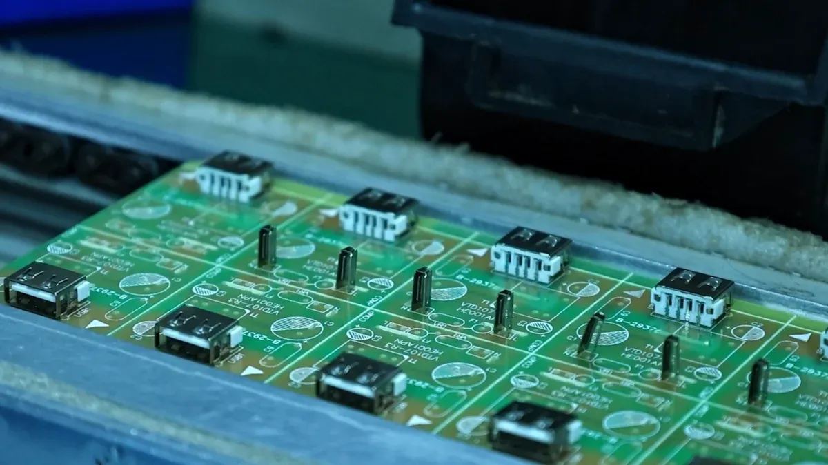
HDI Production Expertise
When you choose LT CIRCUIT for your 10 layer pcb stackup, you gain access to advanced hdi manufacturing. The company uses specialized machines and smart processes to deliver high precision and efficiency for every 10 layer pcb. You can expect a team that works closely with you, converting your Gerber files into the correct format and offering a wide range of options for your hdi pcb stackup. This approach helps you avoid errors and ensures your multilayer pcb stackup meets your exact needs.
Here are some key factors that set LT CIRCUIT apart in hdi production:
Key Factor | Description |
|---|---|
Uses smart manufacturing for high precision in 10-layer pcb stackup. | |
Material Selection | Offers materials that boost performance for hdi pcb stackup designs. |
Quality Control | Applies strict checks to ensure reliable 10 layer pcb results. |
Customization Options | Provides tailored solutions for any multilayer or hdi project. |
You benefit from a skilled team that can spot and solve problems before they affect your 10 layer pcb. This expertise keeps your stackup safe and functional.
Quality and Reliability
LT CIRCUIT uses a full set of quality assurance methods to make sure your 10-layer pcb stackup meets the highest standards. You see this commitment in every step of the hdi pcb stackup process.
Quality Assurance Method | Description |
|---|---|
Automated Optical Inspection (AOI) | Detects defects during production. |
X-ray Checks | Finds hidden internal issues in the stackup. |
Real-time Monitoring with AI Tools | Spots problems early in the 10 layer pcb process. |
Skilled Engineers Monitoring Production Steps | Checks quality at every stage of your hdi pcb stackup. |
Compliance with IPC Standards | Meets industry rules for design and testing. |
Thermal and Stress Testing | Tests 10 layer pcb under tough conditions. |
Supplier Quality Checks | Verifies raw materials for your multilayer pcb stackup. |
SPC, AI Models, Digital Twin Technology | Improves stackup quality and process control. |
LTspice and Monte Carlo Analysis | Checks signal integrity in real-world 10 layer pcb use. |
You can trust the reliability of your 10 layer pcb because LT CIRCUIT tracks important metrics like microvia quality, layer stack capabilities, and industry certifications. This focus on quality gives you confidence in every hdi pcb stackup you order.
Common Pitfalls
Crosstalk Issues
When you design a 10 layer pcb stackup, you must watch for crosstalk between signal lines. Crosstalk happens when signals on one trace affect another, which can cause errors in your hdi circuits. You often see crosstalk in multilayer pcb stackup designs where traces run close together or in parallel. The main causes include capacitive and inductive coupling between adjacent signal lines. Traces that run parallel on the same layer or between layers are especially at risk.
To prevent crosstalk in your hdi pcb, you can:
Avoid routing two parallel wires over long distances on the same layer.
Place ground or power lines between sensitive signal lines.
Use differential signaling for low-swing wiring networks.
Design a ground layer between signal layers to reduce interference.
Tip: Always ensure a continuous return path for signals in your multilayer pcbs. This helps keep your hdi stackup stable and reliable.
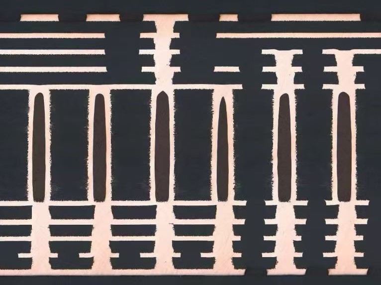
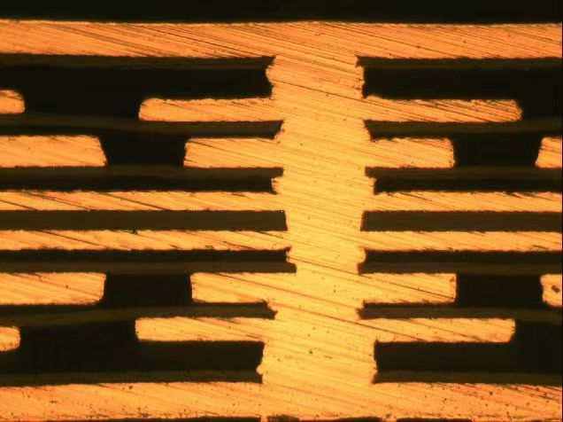
Via Reliability
Vias connect layers in your 10 layer pcb, but they can become weak points if not designed well. In hdi stackup designs, you may face issues like poor plating quality, thermal stress, or high aspect ratios. These problems can lead to cracks or failures in your 10-layer pcb stackup.
You can improve via reliability by following these steps:
Use sequential lamination to reduce stress on vias.
Fill vias properly with conductive or non-conductive epoxy.
Conduct thermal cycling tests from -40°C to 125°C for 1000 cycles to check reliability.
Common Issue | Solution |
|---|---|
Poor plating or voids | Precise drilling and uniform plating |
Thermal stress cracks | Sequential lamination and proper via filling |
Latent defects | Thermal cycling and cross-sectional analysis |
When you follow these best practices, your hdi multilayer stackup will deliver strong performance and long-term reliability.
Reference 10 Layer PCB Stackup
Example Configurations
When you design a 10 layer pcb stackup for hdi projects, you can choose from several proven configurations. Each stackup type supports different needs, such as high-speed signals, mixed analog and digital circuits, or strong power integrity. You should select the arrangement that matches your pcb requirements. Here are some of the most widely used 10-layer pcb stackup options for hdi applications:
Stack-Up Type | Layer Arrangement |
|---|---|
Standard Stack-Up | Top Layer, Signal Layer 1, Internal Power or Ground Plane 1, Signal Layer 2, Internal Power or Ground Plane 2, Signal Layer 3, Internal Power or Ground Plane 3, Signal Layer 4, Internal Power or Ground Plane 4, Bottom Layer |
Mixed Signal Stack-Up | Top Layer (Analog), Signal Layer 1 (Analog), Internal Power or Ground Plane 1, Signal Layer 2 (Digital), Internal Power or Ground Plane 2, Signal Layer 3 (Digital), Internal Power or Ground Plane 3, Signal Layer 4 (Digital), Internal Power or Ground Plane 4, Bottom Layer |
High-Speed Signal Stack-Up | Top Layer, Signal Layer 1 (High-Speed), Internal Power or Ground Plane 1, Signal Layer 2 (Ground Plane), Internal Signal Layer 1 (Signal Integrity), Internal Signal Layer 2 (Signal Integrity), Internal Power or Ground Plane 2, Signal Layer 3 (Ground Plane), Internal Signal Layer 3 (Signal Integrity), Internal Power or Ground Plane 3, Bottom Layer |
Power Integrity Stack-Up | Top Layer, Signal Layer 1, Internal Power Plane 1, Ground Plane, Internal Signal Layer 1 (Power Integrity), Internal Signal Layer 2 (Power Integrity), Internal Power Plane 2, Signal Layer 2, Internal Power Plane 3, Signal Layer 3, Bottom Layer |
Buried Capacitance Stack-Up | Top Layer, Signal Layer 1, Internal Power Plane 1 (with Embedded Capacitance), Signal Layer 2, Inner Power Plane 2 (with Embedded Capacitance), Signal Layer 3, Internal Power Plane 3 (with Embedded Capacitance), Signal Layer 4, Bottom Layer |
Tip: You should always match your hdi stackup to your pcb’s signal and power needs. This helps you get the best performance from your multilayer pcb stackup.
Material Options
You have many choices when selecting materials for your hdi 10 layer pcb. The right material improves signal integrity, thermal stability, and overall reliability. For most hdi stackup designs, FR-4 remains a popular choice because it balances cost and performance. If you need better high-speed or thermal properties, you can use advanced materials like polyimide, BT-epoxy, or cyanate ester. These materials help your stackup handle higher frequencies and tougher environments.
FR-4: Good for general hdi pcb stackup needs.
Polyimide: Works well in flexible or high-temperature multilayer designs.
BT-epoxy: Offers strong thermal stability for demanding pcb projects.
Cyanate Ester: Supports high-speed hdi circuits with low signal loss.
You should always check the dielectric constant and loss factor of your chosen material. This ensures your 10 layer pcb meets the requirements for controlled impedance and signal quality. LT CIRCUIT can help you select the best materials for your 10-layer pcb stackup, so your hdi project succeeds from the start.
You should follow industry standards for 10 layer HDI PCB stackup design:
Principle/Standard | Description |
|---|---|
IPC/JPCA-2315 | Design density estimation models |
IPC-2226 | Microvia and wiring guidelines |
IPC-4104 | Material identification |
IPC6016 | Performance qualification |
LT CIRCUIT uses Laser Direct Imaging, laser-drilled microvias, and strict quality control. You get reliable, high-performance multilayer PCBs that meet your custom needs.
FAQ
What is the main advantage of using a 10 layer HDI PCB stackup?
You get improved signal integrity, better power distribution, and more routing space for complex circuits in your electronic devices.
How do you ensure electromagnetic compatibility in a 10 layer HDI PCB?
You place ground planes between signal layers and use proper shielding. This setup helps you reduce interference and meet electromagnetic compatibility standards.
Which materials work best for high-speed 10 layer HDI PCB designs?
You should choose FR-4, polyimide, or cyanate ester. These materials support high-speed signals and provide strong thermal stability for your stackup.
See Also
Understanding Common Stack-up Configurations for HDI PCBs
Evaluating Costs and Benefits of Advanced HDI PCB Designs
Essential Design Factors for Reliable HDI PCB Production