The Future of HDI Multilayer PCBs and Where the Industry Is Headed
The hdi multilayer pcb industry is expected to experience rapid growth in 2025 and beyond. As demand for 5G, automotive technology, and smart devices increases, the market for hdi multilayer pcb solutions continues to expand. Leading pcb design trends include miniaturization, the use of flexible components, and the adoption of advanced materials. LT CIRCUIT stands out as an innovator in the field. Future developments in pcb design and hdi multilayer pcb technology are set to transform the pcb market.
Key Takeaways
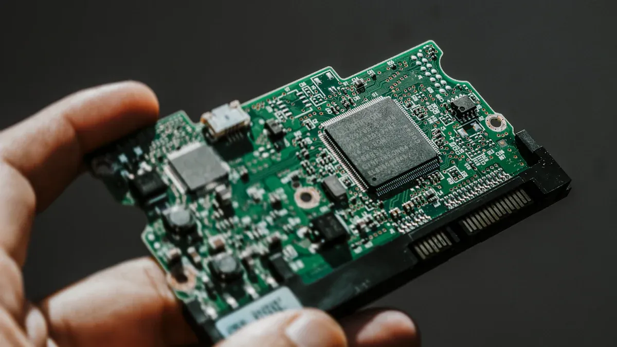
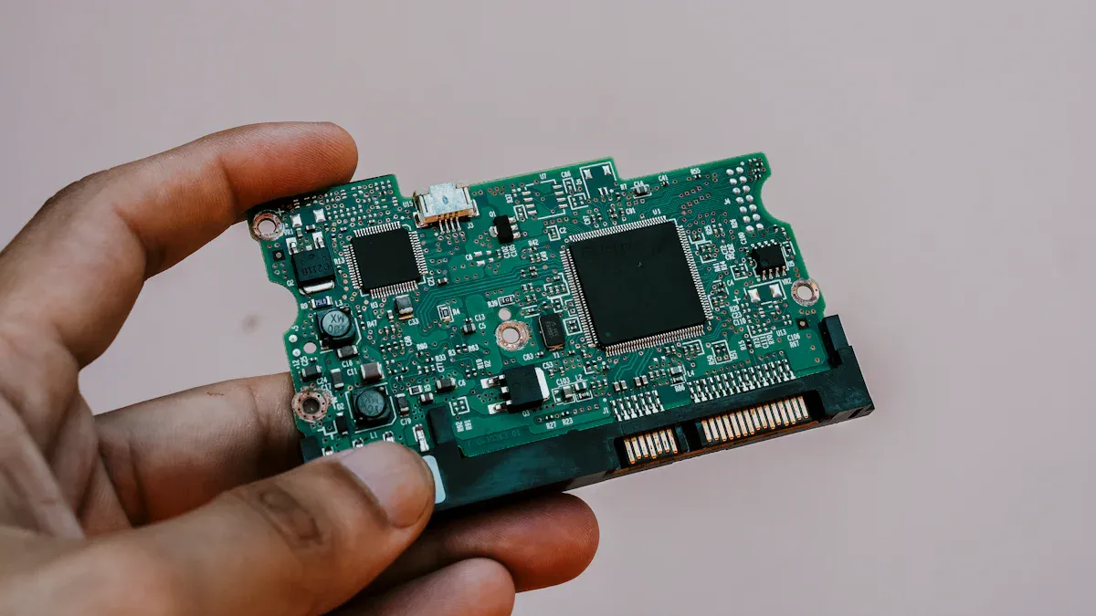
HDI multilayer PCBs are now smaller and stronger. New methods like laser drilling and microvias help this happen. These let more connections fit in a tiny space. This makes devices work better.
Flexible and rigid-flex PCBs help make small, tough devices. These boards can bend and fit into tight spots. They do not break easily. This is good for wearables, medical tools, and smart gadgets.
AI and automation make PCB design and building faster. They help lower mistakes and make better products. This helps companies keep up with the need for fast, reliable electronics in 5G, cars, and medical fields.
Miniaturization Trends
Higher Density Designs
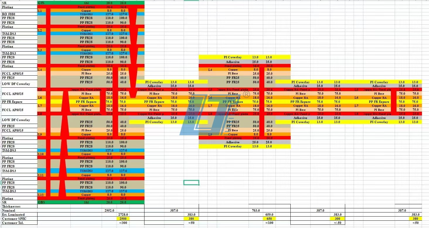
Miniaturization in hdi pcbs means parts are getting smaller. This makes higher density designs very important. Manufacturers use new ways to build these boards. They use laser drilling, multi-layer lamination, and special vias like microvias, blind vias, and buried vias. These methods help make smaller traces and put parts closer together. This helps miniaturization and lets more connections fit in a small space.
Laser drilling makes microvias much smaller than regular vias. This lets more connections fit in the same area.
Multi-layer lamination puts more layers together without making the board bigger.
Via filling and plating make connections between layers stronger and last longer.
High-frequency materials and careful building let traces be thinner and parts be closer.
The table below shows how high-density designs change performance and reliability:
Aspect | Impact on Performance and Reliability |
|---|---|
Size Reduction | Boards can be 30-40% smaller, so devices get tinier. |
Signal Integrity | Shorter connections and thin traces help signals stay strong, even up to 10 GHz. |
Thermal Management | Thermal vias lower heat by 10-15°C, which stops overheating in powerful boards. |
Microvia Design | |
Material Quality | Using low CTE materials keeps vias and traces safe from stress, so boards last longer. |
Manufacturing | Careful building and testing keep boards working for years, with very few failures. |
Design Rules | Smaller traces, smart via spots, and good layer planning help balance size, speed, and how easy it is to make. |
Challenges | More connections make things harder, so microvias and heat control must be done right to keep boards reliable. |
Microvia Innovations
Microvias are a big step forward in pcb design. New microvia technology uses laser drills to make holes as tiny as 20 microns. Boards use even glass materials with low loss, and build up layers one at a time. These things help make thinner, stronger, and better hdi pcbs.
Microvias, blind vias, and buried vias let boards have many layers without getting thicker. Stacked and staggered microvias let more parts fit and use fewer layers. These vias make signal paths shorter, cut down on unwanted effects, and keep signals clear, even at high speeds. Microvia-in-pad designs save space by putting microvias right in the solder pads. This helps make small, high-density electronics.
In the future, pcb design will keep focusing on making things smaller and adding more connections. Microvias and advanced vias will be very important for new devices.
Flexible and Rigid-Flex Integration
Wearables and IoT
Wearable technology and IoT devices keep changing how electronics are made. Rigid-flex pcbs are very important for these new ideas. They mix stiff and bendy parts together. This lets engineers make shapes that old boards cannot do. With flexible pcbs, devices can bend or twist but still work well.
Rigid-flex pcbs give:
Designs that save space in small places.
Fewer connectors and solder joints, so they break less.
Strength to handle shaking, bumps, and lots of movement.
Fast signals, which is needed for smartwatches and trackers.
Materials like polyimide and liquid crystal polymer make boards tough and bendy. These things help make devices smaller and easier to wear. Because of this, smart home gadgets, medical implants, and fitness bands use these special PCBs.
Compact Device Solutions
Today’s electronics need to be tiny and strong. Rigid-flex pcbs help by letting boards fold and fit in small spaces. They also make it easier to put more parts in less room. This is important for medical tools, cameras, and car systems.
Benefit | Impact on Compact Devices |
|---|---|
Space Reduction | Lets boards be packed smaller |
Improved Reliability | Fewer things can go wrong |
Makes devices lighter and easier to use | |
High-Speed Signal Integrity | Keeps signals working in tight spots |
Designers have problems like drilling tiny holes and keeping things cool. They use smart software, laser drills, and machines to check their work. Rigid-flex pcbs help companies make small, strong, and fast electronics for the future.
Advanced Materials in HDI PCB Technology
The electronics industry keeps trying new things with hdi multilayer pcb. Engineers use better materials and new ways to build boards. This helps them make devices that are smaller, faster, and work better. LT CIRCUIT is a leader because they use the newest materials and smart ways to make hdi pcb technology. Their products work well and last long in today’s electronics. They help companies that need top-quality boards.
Low-Loss Dielectrics
Low-loss dielectrics are very important for hdi pcb technology. These materials have a low dielectric constant (Dk) and a low loss tangent (Df). This lets signals move quickly and not lose strength. Devices like 5G phones and network gear need these materials to work right.
Low-loss dielectrics help signals move faster and stay clear. They also let boards be thinner and fit more parts. This helps make electronics smaller and work better.
Property/Benefit | Description/Effect |
|---|---|
Dielectric Constant (Dk) | Low and steady, helps signals move fast and boards be thin |
Loss Tangent (Df) | Low, keeps signals strong and cuts down on noise |
Material Composition | Made with tough PTFE and special resin, stays flat |
Processing Advantages | Works with normal lamination, laser drills fast, no plasma needed for laser vias |
Performance Benefits | Makes PCBs thin, light, and quick; keeps signals strong; lets lines be wider |
Application Compatibility | Works with many laminates, good for fast digital, RF, and microwave PCBs |
LT CIRCUIT picks strong laminates with special resin for their boards. These materials can take heat and stress from modern devices. The right base and copper foil help boards work better with heat and electricity. Conductive ink also helps make tricky circuit shapes that work well. These new materials help with fast and high-frequency uses.
Embedded Components
Putting parts inside the pcb is a big step for hdi pcb technology. Now, engineers can put resistors, capacitors, and chips inside the board. This saves space and makes devices lighter and smaller.
Embedded parts help signals by cutting down on noise and delays.
Putting capacitors close to processors inside the board can lower noise by 30%.
These designs help keep devices cool, even when they run fast.
New ways to build, like laser drilling and stacking layers, make this possible and safe.
Four-layer hdi pcbs with parts inside do a lot in a small space. This matters for cars, planes, medical tools, and phones. LT CIRCUIT uses new materials for fast uses and supports 3d-printed electronics, so their boards are ready for what’s next.
Putting parts inside boards helps make things smaller and work better. It also makes building faster and keeps designs strong.
3d-printed electronics and 3d-printed pcb shapes are used more now. These ways let engineers make even trickier designs and use space better. LT CIRCUIT uses these new ideas to give good answers for every job.
Sustainability in Manufacturing
Green Materials
Manufacturers now try to use green materials for HDI multilayer PCB making. They pick substrates that can be recycled or break down naturally. These choices help cut down waste and make recycling easier when products are old. Many companies, like LT CIRCUIT, use laminates without dangerous stuff inside. They follow strict rules such as the EU RoHS Directive, which bans things like lead, mercury, and cadmium. Soldering without lead, using tin-silver-copper alloys, is now normal. This helps lower heavy metal pollution and keeps the environment safer during making and throwing away.
Water-based inks are now more common. These inks lower VOC emissions by up to 90%. They also make cleaning easier and cut down on chemical waste. New copper recycling methods can get back up to 98% of copper from old PCBs. This saves natural resources and uses less energy than getting new copper from the ground.
Using green materials helps keep the environment clean and lets companies reach world sustainability goals.
Eco-Friendly Processes
Eco-friendly processes are important for lowering the harm PCB making does to the earth. Many factories now use direct metallization instead of electroless copper plating. This change removes bad chemicals like formaldehyde and EDTA. It also saves water and energy, costs less, and makes work safer for people.
Printed electronics are another green way to make things:
They work at lower temperatures, so they save energy.
They do not need electroplating, which uses toxic chemicals.
Conductive inks like silver or carbon work at medium heat and are less toxic.
Recyclable or biodegradable substrates make it easier to take apart and reuse materials.
These ways help with circular design and cradle-to-cradle life cycles.
Manufacturers keep using these new ideas, making HDI multilayer PCBs better for the planet in the future.
AI and Automation
Design Optimization
Artificial intelligence is changing how engineers design HDI multilayer pcb. AI tools now do many boring jobs for engineers. These tools help pick the best spots for parts. They can also guess where signal problems might happen. Machine learning can make trace lines shorter by about 20%. This helps signals move faster and keeps devices working well. AI checks if design rules are broken, like if microvias are too close. It gives quick ideas to fix these problems. This means engineers do not have to redo work as much. It also makes the design process up to 30% faster.
AI software also helps keep signals and power strong. It can spot problems like crosstalk or impedance mismatches. Then it tells engineers how to fix them so signals stay clear. AI helps with heat by looking at hot spots and telling where to put vias or what materials to use. This can lower heat resistance by about 25%. These smart tools make pcb layouts better and more reliable. They are very helpful for fast things like 5G and 3d-printed electronics.
AI-driven pcb design automation lets engineers make better boards faster. There are fewer mistakes and the boards work better.
Smart Production
Automation in pcb factories makes products better and more reliable. Automated optical inspection and x-ray systems find problems fast and correctly. These machines look for open circuits, shorts, and issues with buried or blind vias. Laser drilling makes microvias as tiny as 50 microns. This is needed for tricky multilayer pcb.
Modern factories use clean rooms to keep dust away. They use special plating to make copper layers even. Sequential lamination adds layers to make boards strong and reliable. Automated tests, like flying probe and impedance tests, check every pcb to make sure it is good. These smart ways of making things help new tech like 3d-printed pcb and 3d-printed electronics. They make sure every board works well in real life.
Automation and AI in pcb production help companies make great products. These products meet the needs of today’s fast-changing technology.
Market Drivers for HDI Multilayer PCB
5G and AI Applications
The hdi multilayer pcb market is growing fast. This is because 5G and AI are used more now. Many companies want smaller and faster electronics. They also want devices that work well and do not break easily. This makes people need better pcb solutions. 5G networks need to send data quickly and keep signals strong. AI and IoT also need circuit boards that work fast and well. These changes make the market want smaller and more advanced designs.
Making things smaller and better helps more people use hdi multilayer pcb.
Smart devices like phones, tablets, and wearables need small and powerful pcbs.
Upgrading 5G networks makes more people want new pcb technology.
Flexible and rigid-flex pcbs are used a lot in medical and wearable gadgets.
New ways to build, like laser drilling and new materials, help the market grow.
LT CIRCUIT is a leader in making new hdi multilayer pcb for these fast-growing areas. The company always works hard to make good products. Their smart ways of making things help them stay ahead of others.
Automotive and Medical
Cars and medical tools also help the hdi multilayer pcb market grow. In cars, things like driver-assist, electric engines, and screens need strong and tiny pcbs. These boards must work in tough places and be very safe. Microvias and new materials make boards last longer and work better.
Sector | Key Applications | Market Impact |
|---|---|---|
Automotive | ADAS, EV powertrains, infotainment | Miniaturization, reliability, speed |
Medical | Imaging, monitoring, surgical, lab analysis devices | Portability, precision, intelligence |
Medical devices use multilayer pcb to be smaller and do more things. This helps patients feel better and makes devices work well. LT CIRCUIT keeps making new things to help car and medical markets. The hdi multilayer pcb market will keep growing as these fields get better.
Challenges and Opportunities
Technical Barriers
The HDI multilayer PCB industry has many tough problems to solve. Companies need to buy special machines and hire skilled workers. This makes making boards cost more money. Building high-density boards is hard and needs experts in electronics, materials, and chemistry. Even tiny mistakes in drilling or plating can cause fewer good boards and slow down the supply chain. Companies must follow strict rules to make sure every board works well.
Key technical problems are:
Making boards costs a lot because of special tools and workers.
High-density layouts are hard to design and build.
Problems in the supply chain can make it hard to get materials.
Strict checks are needed to keep boards reliable.
Companies must always find new ways to meet what the market wants.
Technical Barrier | Description & Impact |
|---|---|
High Layer Count Structure | Layers must line up right or signals will have trouble in AI and 5G devices. |
Microvia Laser Drilling | Needs careful control so holes are good and drilling works well. |
Thermal Management | Materials must match copper’s growth so boards do not break when heated. |
Starting a factory costs a lot, sometimes millions of dollars. Small companies may have a hard time using smart factory ideas, but these are needed to stay in the game.
Growth Potential
Even with these problems, the HDI multilayer PCB market can grow a lot. People want smaller and better electronics more than ever. Cars, planes, and phones need advanced boards for electric cars, 5G, and smart gadgets. New ideas like Any-Layer HDI, putting parts inside boards, and very thin copper let boards be smaller and stronger.
More IoT and smart gadgets mean we need more complex boards.
Using AI in design and making boards helps make things faster and better.
Green rules make companies use safer materials and ways to build.
Governments in places like Asia-Pacific give help to start new factories.
When PCB makers and OEMs work together, they can make new boards and custom designs faster. Using robots and AI helps check boards and makes them quicker to finish. As technology gets better, companies like LT CIRCUIT can keep leading with new ideas and meet what the market needs.
UHDI, putting parts inside boards, and using eco-friendly ways are important for the future of pcb design.
LT CIRCUIT is very good at hdi pcb technology and always checks quality to help new ideas grow.
Companies do better when they work with top groups who keep up with new pcb changes and technology.
Learning about new pcb design trends helps companies keep winning in a fast-changing market.
FAQ
What makes HDI multilayer PCBs different from standard PCBs?
HDI multilayer PCBs have microvias and special materials. These boards let more parts connect in less space. Devices can be smaller and work faster with these boards.
How does LT CIRCUIT ensure product quality?
LT CIRCUIT checks every board with strong tests and good machines. They use top materials so each board is safe and works well.
Which industries benefit most from HDI multilayer PCBs?
Industry | Key Benefit |
|---|---|
Automotive | Very dependable |
Medical | Makes things smaller |
5G/AI | Sends data very quickly |
These fields use HDI PCBs for smart features and small designs.
See Also
Designing And Producing HDI Multi-Layer PCBs Explained
Explore Cutting-Edge HDI PCB Prototyping Methods Now
Evaluating Costs And Benefits Of Advanced HDI PCB Tech