Advanced Blind & Buried Hole PCB Design Skills
Advanced blind & buried hole skills help engineers make dense PCB layouts. Blind vias join outer layers to inside layers. Buried vias connect only inside layers. These methods lower signal problems and help with routing. Keeping enough space between vias and traces stops short circuits. It also keeps signals strong. Makers use careful drilling and plating for good results. Designers must keep designs simple enough to build. Tighter spaces cost more and need better tools.
Key Takeaways
Blind and buried vias help PCB design. They let you make more connections in a small space. This makes boards smaller and lighter. Good via placement and aspect ratio control are important. They keep signals strong and lower interference in fast circuits. Engineers and fabricators should work together early. This helps make boards easier to build and have fewer errors. Picking the right layer stack-up and via types is important. It can make heat and electricity move better. This helps the board work well. Using rules like IPC-2221 and IPC-6012 is smart. These rules help keep advanced PCB designs good and reliable.
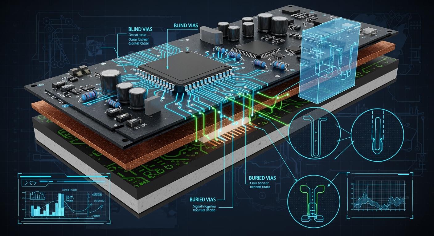
Blind & Buried Hole PCB Concepts
Blind Vias vs. Buried Vias
Blind vias and buried vias are important in multilayer pcb designs. Blind vias link an outside layer to one or more inside layers. They do not go through the whole board. Buried vias only connect inside layers. You cannot see them from the outside. Microvias are even smaller than blind or buried vias. They help with very tight routing and tiny parts. The table below shows how blind and buried vias are different:
Type of Via | Definition | Visibility from Outer Layers | Advantages |
|---|---|---|---|
Blind Via | Connects an external layer to one or more inner layers, not passing through the board. | Not visible | Saves space, enables compact designs, improves signal integrity by reducing signal path length. |
Buried Via | Located entirely within the PCB, connecting only inner layers. | Not visible | Allows outer layers to be used for other purposes, such as component placement or routing. |
Microvias make routing even denser. They let designers use shorter paths. They also work well for via-in-pad designs in fast and RF circuits.
Role in High-Density PCB Design
Blind and buried hole technology is very important in new pcb designs. These vias let engineers fit more connections in less space. This helps make boards smaller and lighter. Designers can use these vias to build compact layouts. The table below lists the main benefits:
Advantage | Explanation |
|---|---|
Higher Routing Density and Smaller Form Factor | Enables efficient layer-to-layer connections in compact layouts, allowing for smaller, lighter PCBs. |
Better Thermal and Electrical Performance | Improves conductivity by minimizing distance between layers, reducing signal interference. |
Minimized Signal Delay and Parasitics | Reduces signal travel distance, minimizing delays and parasitic effects critical for high-speed circuits. |
Buried vias make signal paths shorter. This helps signals move faster between parts. They also cut down on layer jumps. This keeps signals strong in fast circuits.
Note: Buried vias are very useful in RF pcb design. They give hidden connections that help with ground stitching. They also keep impedance steady in boards with many layers.
When to Use Each Via Type
Designers pick blind or buried vias for different needs. Blind vias are good when space is tight and routing is dense. They save space and keep performance high. Buried vias are best in boards with many layers. They free up the outside layers for parts or more routing. In small spaces, like under BGAs, both types are needed. This helps with routing and keeps signals strong. Microvias are best for very dense layouts and tiny parts. But they need special tools to make.
Advanced PCB Design Skills for Vias
Layer Stack-Up for Blind & Buried Vias
Engineers need to plan the layer stack-up with care. The stack-up decides how vias connect layers. It also affects how strong the pcb is. A good stack-up helps control heat and keeps the board flat. Symmetric stacks stop the board from bending. They also make drilling easier. The thickness between layers sets how deep each via goes. This matters for both blind and buried vias.
The table below shows usual values for stack-up:
Parameter | Standard Value | Minimum Value |
|---|---|---|
Via Diameter | 4–6 mil | 3 mil |
Pad Diameter | 8–12 mil | 6 mil |
Aspect Ratio | 1:1 | 1.2:1 |
Dielectric Thickness | 4–20 mil | 2 mil |
Copper Thickness | 0.5–2 oz | 0.5 oz |
Clearance (Via to Via) | 4 mil | 3 mil |
Clearance (Via to Trace) | 4 mil | 3 mil |
Solder Mask Opening | ≥2 mil larger than pad | ≥1 mil larger |
Tip: Planning the stack-up is very important. It helps match how the board expands with heat. It also keeps the board strong during making.
Designers should pick substrates with Tg of 170°C or more. This lets the board handle heat during use. Following IPC-2221 and IPC-6012 standards helps meet quality rules.
Vias Selection and Placement
Choosing the right via type and placing it well is key. Blind vias start at the outside and end at an inside layer. This saves space on the board. Buried vias connect inside layers only. They help with tight routing and do not use surface space. Both types are used in high-density designs.
The table below compares how via types affect boards:
Via Type | Impact on Performance | Impact on Manufacturability |
|---|---|---|
Blind Vias | Improve signal strength, remove stubs | Make boards harder and cost more |
Buried Vias | Help inner routing, keep surface clear | Make boards harder and cost more |
Through Vias | Good conductivity, but make stubs | Easier and cost less |
When placing vias, engineers should:
Keep at least 3.5 mil space between blind vias and pads.
Make pad size 2–3 times bigger than the via opening.
Do not put blind via openings under surface mount pads.
Connect blind vias only between layers next to each other.
Note: Picking and placing vias well helps performance. It also makes boards easier to build.
Signal Integrity with Blind Vias
Signal strength is very important in modern electronics. Blind vias can make signal paths shorter. This helps signals stay strong and cuts down stubs. But bad design can cause problems. Blind vias may create shapes that mess up signals at some frequencies. This can cause signal loss and crosstalk, especially in multilayer pcb designs.
For fast designs, keep blind via aspect ratio between 0.75:1 and 1:1. This stops problems like uneven plating and high resistance. These issues can hurt signal strength. Putting vias too close can cause crosstalk and reflections. This is worse when signals are faster than 1 GHz. Longer vias can make signals weaker, losing 3–5 dB in the worst cases.
Tip: Careful via placement and aspect ratio control are needed. They help keep signals strong and boards working well.
Manufacturability Considerations
Making advanced vias needs strict process control. Blind and buried vias need more drilling and lamination steps. This makes boards cost more to build. Engineers must know these costs when planning projects.
Key process controls include:
Sequential Lamination: Adds more layers but keeps boards thin.
Drilling Techniques: Using machines or lasers changes via quality and cost.
Plating Processes: Right plating thickness is important for buried vias.
Quality checks are important:
X-ray checks inside for bad or misaligned buried vias.
Microsectioning lets engineers look at via quality under a microscope.
Electrical tests make sure all vias work well.
Thermal imaging finds problems by watching heat during tests.
The table below lists common process problems and fixes:
Key Process Control Parameter | Associated Challenges | Solutions |
|---|---|---|
Laser drilling accuracy | Small via diameter (≤0.1 mm) | Incomplete or misaligned vias |
Via bottom quality | Resin residue or roughness | Poor copper adhesion |
Copper filling consistency | Uneven plating or voids | Reliability failure |
Thermal stress | CTE mismatch across layers | Via cracking |
Yield control | Defect accumulation across steps | Increased scrap rate |
Note: Following strict process controls and standards keeps quality high. It also makes blind & buried hole pcb designs last longer.
Overcoming Challenges in Blind & Buried Hole Design
Preventing Manufacturing Defects
Blind & buried hole PCB designs can be hard to make. These designs often have more mistakes because they need careful drilling and many lamination steps. Engineers use different ways to stop these problems:
Placing parts in smart spots makes routing easier and cuts down on interference.
Designing vias well, like keeping a good annular ring and not using too many in fast signal paths, helps avoid mistakes.
Balancing copper keeps copper spread out evenly. This stops the board from bending and helps with heat.
Following spacing rules lowers the chance of shorts and other problems.
Adding ways to handle heat keeps parts safe from getting too hot.
Working carefully and as a team helps keep boards high quality and lowers mistakes.
Managing Cost and Complexity
Blind and buried vias make boards more complex and cost more to build. These methods need tighter controls and extra steps, like special lamination and careful drilling. To save money, engineers:
Only use as many blind via sets as needed.
Pick via sizes and spacing that match the usual 4–6 mil size.
Use even stackups and standard thicknesses to fit factory tools.
These choices help keep routing tight but costs lower. Testing and checking for quality also cost more, but they are needed to make boards last longer.
Ensuring Reliability and Testability
Reliability is very important in small, crowded electronics. Engineers use different checks to see if vias work well:
Metric | Description | Impact on Reliability |
|---|---|---|
Aspect Ratio | Depth to diameter ratio of the via | High ratios can cause uneven plating and failures |
Manufacturing Limits | Fabrication constraints affecting via performance | Poor management increases plating challenges |
Design Adjustments | Changes to improve via performance | Larger drill diameters improve reliability |
To make sure boards work well, engineers do CAM and DFM checks, look at the stackup, and test with electricity. They also check for bending in thin boards with lots of BGAs. These steps help keep blind & buried hole PCB boards strong and working for a long time.
Best Practices for Blind & Buried Vias
Working with Fabricators
Blind & buried hole pcb projects work best when engineers and fabricators talk early. They need to agree on the stack-up and say where each via starts and ends. Early talks help pick prepreg that lets resin fill vias better. Engineers should use IPC-2221 rules for via size and layout. This makes sure the board is easy to build and works well. Buried vias should not overlap. This makes lamination steps easier and less tricky. Nesting spans instead of crossing them helps with plating. Fabricators like to use alignment pins during lamination. This keeps layers lined up and stops mistakes. Controlled-depth drilling for blind vias stops holes from going too deep. This keeps the board strong. Following IPC-6012 rules helps the board last longer.
Tip: If engineers and fabricators work together early, the board is easier to make and needs fewer changes.
Using EDA Tools Effectively
Modern EDA tools help engineers handle blind, buried, and microvias. Design Rule Check (DRC) finds spacing problems and checks via spots. Placement tools help fit parts on the board and make routing easier. Automation in EDA tools can suggest stack-ups and materials. This helps make boards smaller and keeps signals strong. Engineers should keep via aspect ratio at 10:1 or less. Via sizes should be between 0.15 mm and 0.2 mm. Good spacing between vias and pads stops problems during making. Simulation tools show how signals move. This helps stop crosstalk and keeps signals clear in fast boards.
Documentation and Communication
Clear paperwork and good talking are needed for making boards right. Engineers should use IPC-2221, IPC-2581, and IPC-6012 to share needs for blind, buried, and microvias. Good files and keeping track of changes help with quality. Talking between design and making teams lets them fix things fast. This makes moving from design to making smoother. These steps lower mistakes, speed up testing, and help boards last longer.
Standard | Description |
|---|---|
IPC-2221 | General PCB design, layout, and performance guidelines |
IPC-2581 | Data exchange for fabrication and assembly |
IPC-6012 | Rigid PCB quality and qualification standards |
J-STD-001 | Soldering requirements for electronics assembly |
ISO 9001 | Quality control for manufacturing processes |
Note: Good paperwork and early talking help meet all needs for advanced via types. This keeps boards high quality and reliable.
Engineers can get good at blind and buried hole pcb design by doing these things:
Keep aspect ratios at 1:1 or less. This makes vias strong.
Use a drill size of at least 0.15 mm for blind vias.
Plan layer stack-ups so there is no interference.
Keep at least 0.2 mm space between features.
Place vias to help signals in fast designs.
Working with manufacturers often makes boards more reliable. The table below shows how teamwork helps:
Aspect | Blind Vias Benefit |
|---|---|
Electrical Performance | Better impedance and less return loss |
Signal Integrity | Works well at high frequencies |
Mechanical Strength | Stays strong when stressed |
FAQ
What is a rigid-flex pcb and how does it differ from standard boards?
A rigid-flex pcb has both stiff and bendable parts in one board. This lets engineers fold or bend the board as needed. Rigid-flex pcb designs help save space and make devices stronger. They work well when things need to be both tough and flexible.
Why do engineers use rigid-flex in high-density interconnect designs?
Engineers pick rigid-flex for high-density interconnects to fit more circuits in tight spots. Rigid-flex pcb technology lets them make tricky layouts. It helps connect parts that move while keeping signal paths short and strong.
How does rigid-flex pcb help with structural integrity?
Rigid-flex pcb designs make devices stronger by joining stiff and bendy parts. This helps the board handle shaking and bending. Devices with rigid-flex pcb can move many times without breaking wires.
Can rigid-flex pcb support multilayer pcbs and signal integrity management?
Yes, rigid-flex pcb can have many layers. Designers use rigid-flex to stack layers and keep signals clear. Signal integrity is better because rigid-flex pcb cuts down on noise and keeps signals strong.
What are the main benefits of using rigid-flex pcb in modern electronics?
Rigid-flex pcb gives many good things. It saves space, makes devices lighter, and allows cool shapes. Rigid-flex pcb also means fewer connectors are needed. Devices work better and last longer with rigid-flex pcb.
See Also
Essential Skills for Designing Multi-Layer PCB Layouts Effectively
Overcoming Manufacturing Hurdles with Buried Via Technology in PCBs
Explore Cutting-Edge Techniques for HDI PCB Prototyping Now
Enhancing Space and Efficiency with Blind Via Technology in PCBs
Perfecting Immersion Tin Finishing Techniques for PCB Designs