What Are the Most Advanced Materials Used in HDI PCB Manufacturing
You see advanced fr4 materials, polyimide, BT-epoxy, ABF, RCC, and PTFE leading HDI PCB innovation.
FR4 holds 31.8% market share, showing dominance in printed circuit boards.
Advanced fr4 materials provide strong electrical, mechanical, and thermal properties.
Advanced fr4 materials, thin copper foils, ultra-smooth copper, laser-drillable glass, spread glass, ENIG, and LPI solder mask support miniaturization and reliability.
LT CIRCUIT uses advanced fr4 materials to deliver advanced hdi materials pcb for high-density applications.
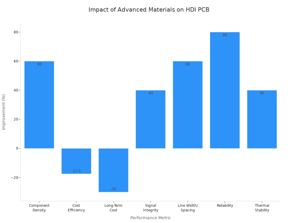
Metric | Improvement/Impact |
|---|---|
Reliability | Failure rates drop to 0.02% |
Line Width/Spacing | 50μm, area reduced by 60%, thickness by 40% |
Thermal Stability | 40% fewer failures in high-temp environments |
Key Takeaways
Advanced materials like FR4, polyimide, and BT-epoxy enhance the performance of HDI PCBs, providing better electrical, mechanical, and thermal properties.
Choosing the right dielectric materials is crucial for achieving higher speeds and improved reliability in printed circuit board designs.
Utilizing ultra-smooth copper foils is essential for minimizing signal loss in high-frequency applications, ensuring optimal performance in advanced HDI PCBs.
Advanced HDI Materials PCB
Dielectric and Insulating Materials
You encounter dielectric materials at the heart of every advanced hdi materials pcb. These specialized materials separate conductive layers and control signal speed, loss, and reliability. Engineers select advanced materials like polyimide, BT-epoxy, ABF, RCC, and PTFE for their unique electrical, thermal, and mechanical properties.
Tip: Choosing the right dielectric materials helps you achieve higher speeds and better reliability in your printed circuit board designs.
Here is a table showing how dielectric materials differ by speed and loss:
Category | Distinguishing Properties | Example Materials |
|---|---|---|
Normal speed and normal loss | Higher dielectric loss, suitable for 0 to 5 GHz, Df > 0.012 | EM-827(I), EM-370(Z), Nelco N7000-2HT |
Medium speed and medium loss | Flatter Dk response, suitable for 0 to 10 GHz, Df 0.012 to 0.007 | FR408HR, Isola I-Speed |
High speed and low loss | Lower dielectric loss, suitable for 10 to 30 GHz, Df 0.0095 to 0.0022 | EM-528, I-Tera MT40, Megtron6 R-5775 |
Very high speed and very low loss | Flattest Dk response, suitable for 20-60 GHz, Df ≤ 0.0021 | EM-890K, Isola Tachyon 100G, Astra MT77 |
PTFE stands out for high-frequency signals. You use it when you need low dielectric constant and dissipation factor, which supports signal speeds up to 10 GHz. Polyimide works best for flexible and durable applications, such as multilayer flex PCBs. BT-epoxy offers moisture resistance and dimensional control. ABF enables ultra-fine line etching and laser drill compatibility. RCC provides a lower-cost option with reasonable thermal performance.
Material | Dielectric Constant (Dk) | Dissipation Factor (Df) | Glass Transition Temperature (Tg) | Coefficient of Thermal Expansion (CTE) |
|---|---|---|---|---|
BT Epoxy | < 4.0 | ~0.010 | 180–200°C | N/A |
ABF | 3.0–3.3 | < 0.008 | > 210°C | < 45 ppm/°C |
Polyimide | N/A | N/A | N/A | 20-40 ppm/°C |
RCC | N/A | N/A | N/A | N/A |
You see advanced hdi materials pcb used in medical devices, aerospace, automotive electronics, and 5G infrastructure. LT CIRCUIT selects advanced pcb materials for each application, ensuring high performance and reliability.
Recent trends include the use of LCP and ceramic substrates for 5G and high-frequency applications. Embedded components within PCB layers help you reduce board size and improve electrical performance.
Copper Foils
Copper foils form the conductive pathways in every advanced hdi materials pcb. You choose between thin copper foils and ultra-smooth copper based on your signal integrity and frequency needs.
Feature | Thin Copper Foils | Ultra-Smooth Copper |
|---|---|---|
Signal Integrity | Moderate, suitable for standard applications | High, minimizes signal loss and distortion |
Manufacturing Compatibility | Versatile and cost-effective | Higher cost, may not always be necessary |
Frequency Performance | Adequate for standard frequencies | Optimal for high-frequency applications |
Cost Considerations | Generally lower cost | Higher cost due to processing requirements |
Thin copper foils allow you to create finer lines and tighter spacing, which supports miniaturization. Ultra-smooth copper improves signal integrity, especially in high-frequency designs. LT CIRCUIT uses both types to match your application requirements, from consumer electronics to aerospace avionics.
Note: Ultra-smooth copper is essential for advanced hdi materials pcb in 5G and high-speed server storage, where signal loss must be minimized.
Reinforcement Materials
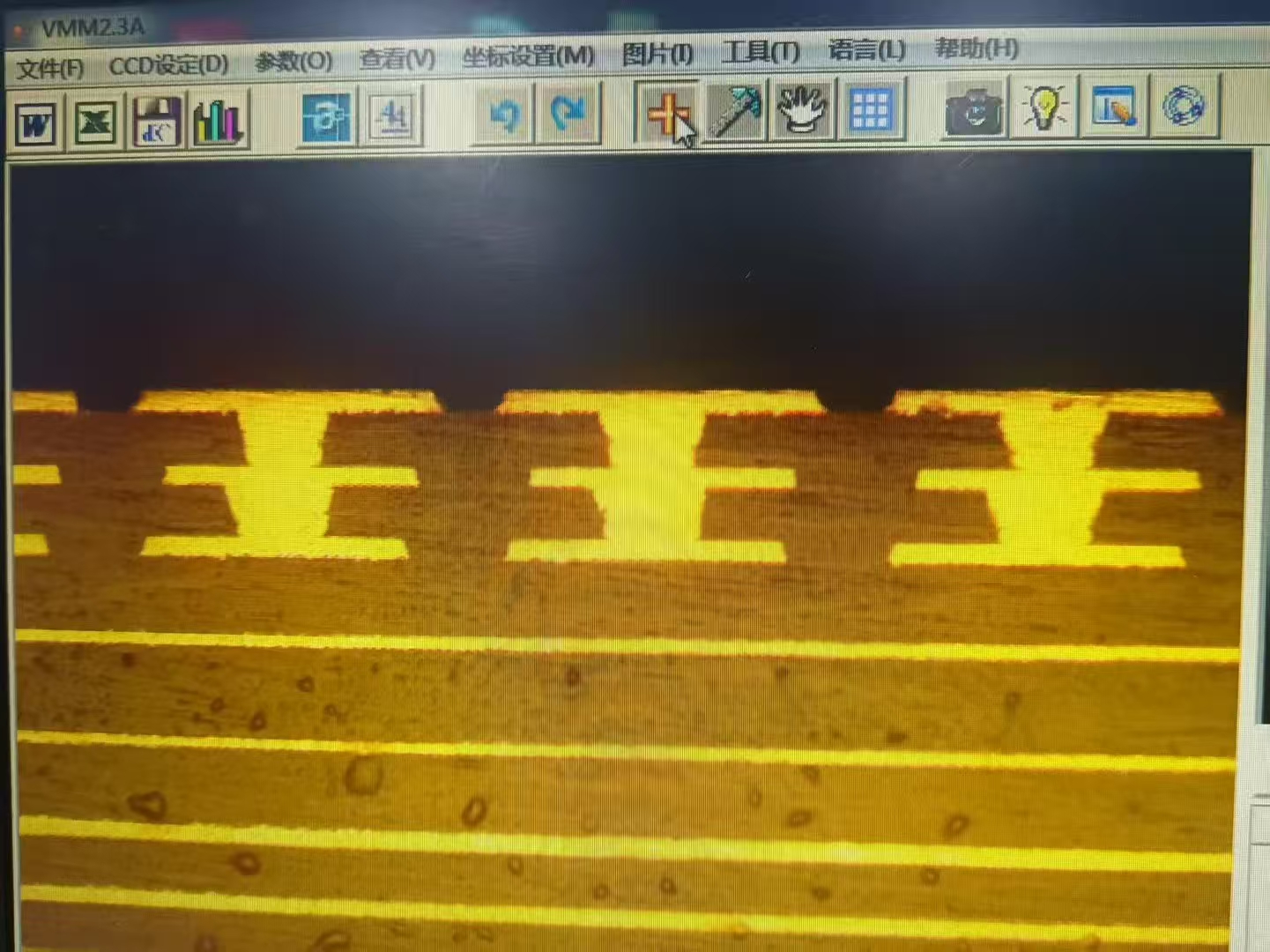
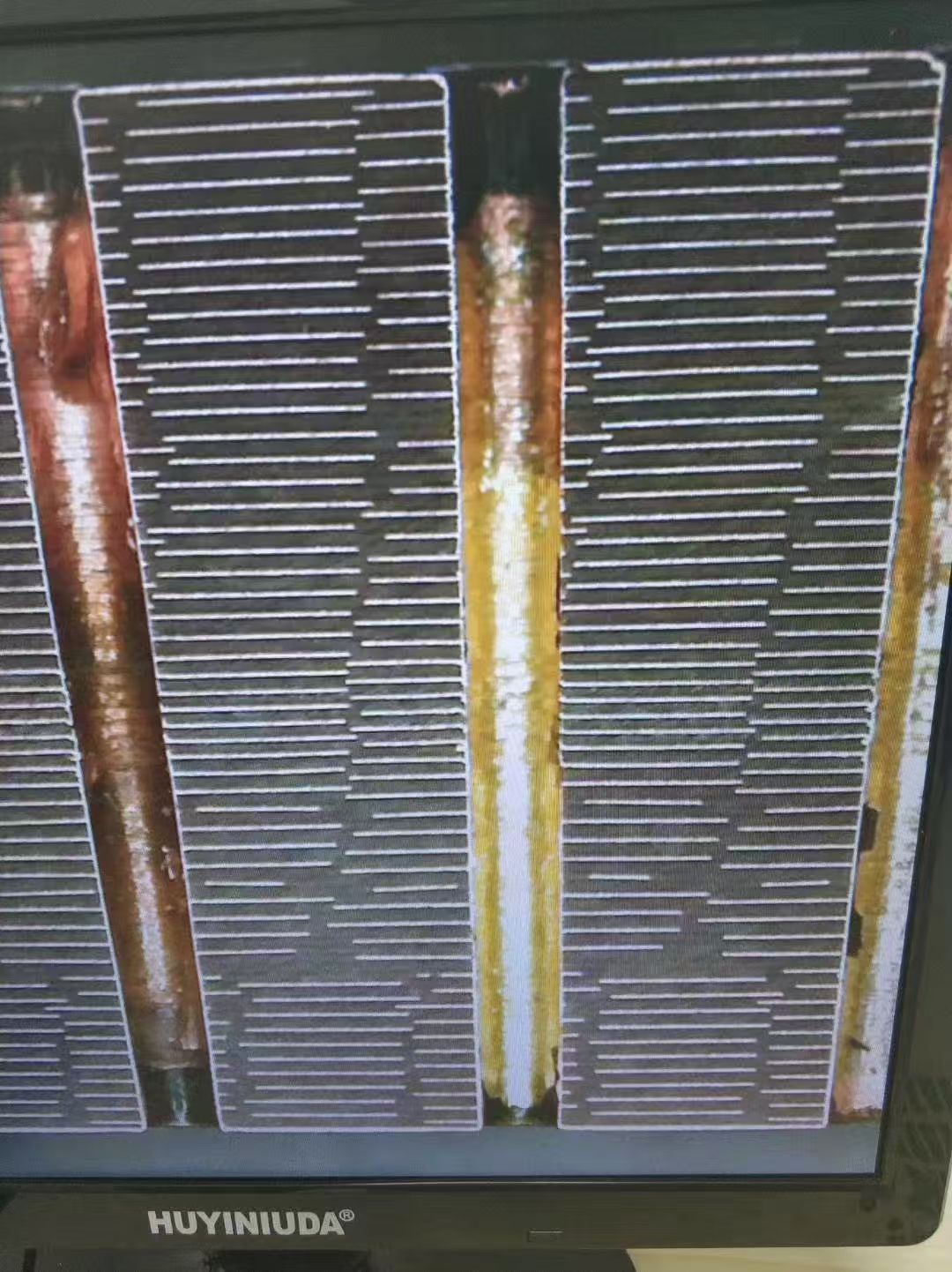
Reinforcement materials give your printed circuit board strength and stability. You find glass weaves, laser-drillable glass, and spread glass in advanced hdi materials pcb. These specialized materials support microvias and fine-pitch designs.
Laser-drillable dielectrics use spread yarns for a uniform fabric, which reduces drilling problems.
Laser drilling technology lets you control drilling depth and size, making microvias possible.
Microvias formed by laser drilling are crucial for interconnections in high-density devices.
LT CIRCUIT applies advanced pcb materials and reinforcement techniques to meet the demands of harsh environments. For example, oil rig sensors use PTFE substrates and rolled copper to operate reliably for years. Aerospace avionics rely on ceramic-filled laminates and hard gold plating for zero failures in orbit.
Sustainability tip: You can choose eco-friendly reinforcement materials and recyclable copper to reduce environmental impact.
You see advanced hdi materials pcb in medical devices, automotive electronics, and 5G infrastructure. These sectors benefit from the reliability and compact design that specialized materials provide.
HDI PCB Manufacturing and Material Selection
Surface Finishes and Solder Masks
You play a key role in choosing the right surface finishes and solder masks during hdi pcb manufacturing. These choices affect the reliability and performance of high density interconnect boards. Surface finishes protect copper traces and ensure good solderability. You often see ENIG, immersion silver, ENEPIG, and immersion tin used in microvia pcb manufacturing.
Surface Finish | Recommended Application | Key Advantages |
|---|---|---|
ENIG | High-frequency signals | Superior conductivity, corrosion resistance |
Immersion Silver | RF, automotive, consumer | Smooth surface, minimal signal distortion |
ENEPIG | High-density, RF circuits | High reliability, strong adhesion |
Immersion Tin | High-density interconnects | Reliable solderability, consistent finish |
ENIG gives you excellent surface flatness, which is ideal for fine-pitch and high-speed digital interfaces. Immersion silver provides a smooth surface, reducing signal loss in microvia pcb manufacturing. ENEPIG offers strong adhesion, which is important for high-density interconnect designs. Immersion tin ensures reliable soldering for dense layouts.
You also need to select the right solder mask. Liquid Photo-Imaginable (LPI) solder masks allow you to achieve finer resolution and better alignment. Laser Direct Imaging (LDI) technology helps you cover tiny pads and leave gaps for soldering. High dielectric properties in solder masks minimize signal interference, which is critical for applications of hdi pcbs in automotive and aerospace.
Tip: High-resolution LPI solder masks help you avoid defects like solder bridging and shorts, especially when component density is high.
Advanced Materials Comparison
You must compare advanced engineered pcb materials to find the best fit for your project. Dielectric constant (Dk), dissipation factor (Df), and glass transition temperature (Tg) are important properties. High-performance laminates with low Dk and Df support high-speed digital interfaces and microvia pcb manufacturing.
Dielectric materials for high-speed applications have Dk ≤3.5, which supports signal integrity in microvia pcb manufacturing.
Standard FR-4 materials have Dk ≥4.5, which can cause losses above 10GHz.
High Tg values (170°C or higher) prevent warping during soldering and thermal cycling.
Advanced uhdi build-up films and ceramic-filled polymers offer ultra-low loss and high thermal reliability.
Factor | ENIG | HASL | Immersion Silver |
|---|---|---|---|
Cost | High | Low | Moderate |
Surface Flatness | Excellent | Poor | Excellent |
Solderability | Excellent | Excellent | Excellent |
Shelf Life | 12+ months | 12 months | 6-12 months |
Thermal Resistance | Moderate | Good | Good |
Applications | HDI, fine-pitch | General-purpose | HDI, high-speed |
You see that ENIG is preferred for high-reliability and fine-pitch microvia pcb manufacturing. HASL works well for general-purpose boards but is not suitable for high component density. Immersion silver balances cost and performance, making it useful for high-speed and high-density interconnect designs.
Note: Advanced materials like polyimide, BT-epoxy, and resin-coated copper (RCC) improve throughput and reduce drilling time in microvia pcb manufacturing. These materials also support multilayer stackups and high component density.
Selection Tips
You need practical tips to select the right materials for hdi pcb manufacturing. Start by defining your application needs. If you work with high-frequency or high-power designs, choose materials with low Dk and Df. For boards with many layers, select materials with low CTE to avoid warping.
Identify your application: High-frequency, high-power, or thermally challenging environments require special materials.
Consider layer count: Boards with 10+ layers need low CTE materials for reliable multilayer stackups.
Evaluate signal integrity: Use low-loss materials for high-speed digital interfaces and microvia pcb manufacturing.
Balance cost and performance: Advanced engineered pcb materials offer benefits of hdi pcbs, but you should assess if the extra cost fits your project.
Test compatibility: Make sure your laminate works with your manufacturing process.
You can also choose halogen-free or eco-friendly options for long-term compliance. RCC helps you improve throughput and supports dense microvia pcb manufacturing. Staggered microvias increase reliability, especially in boards with high component density.
LT CIRCUIT gives you access to customization options, including different surface finishes, solder mask colors, embedded components, and stack-up design assistance. You benefit from advanced manufacturing techniques like laser direct imaging, microvia drilling, and automated inspection. LT CIRCUIT uses tiered testing strategies, including X-ray inspection, microvia stress testing, and environmental testing, to ensure the reliability of advanced engineered pcb materials.
Callout: Collaboration between design and manufacturing teams helps you avoid common defects like delamination, misalignment, and via defects. Quality assurance and thorough testing are essential for reliable microvia pcb manufacturing.
You improve HDI PCB performance when you choose advanced materials. LT CIRCUIT helps you achieve reliable, compact, and high-speed designs. See how material selection benefits your application:
Application Area | Key Benefits |
|---|---|
Telecommunications | Low loss, thermal management |
AI/Data Processing Systems | High speed, compact design |
Industrial Control Systems | Miniaturization, reliability |
Consult LT CIRCUIT for expert advice on HDI PCB design.
FAQ
What makes HDI PCB materials different from standard PCB materials?
You find HDI PCB materials offer better electrical performance, higher thermal stability, and support for finer lines. These features help you achieve miniaturization and reliability.
How do you select the right material for your HDI PCB project?
You start by considering your application’s speed, temperature, and reliability needs. You compare dielectric constants, loss factors, and thermal ratings to match your requirements.
Can advanced HDI materials improve signal integrity in high-frequency designs?
You see advanced materials like ultra-smooth copper and low-loss dielectrics reduce signal loss. These choices help you maintain signal integrity in high-frequency circuits.
See Also
Explore Cutting-Edge Techniques for HDI PCB Prototyping
Understanding the Design and Production of Any Layer HDI PCBs
Identifying Top Materials for Designing High-Speed PCBs