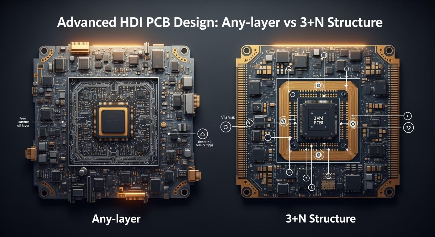
Advanced HDI PCB Design: Any-layer vs 3+N Structure
You must pick between Any-layer or 3+N structure in Advanced HDI PCB Design. Each choice changes how you manage signal quality, reliability, and cost. Stacked microvias make boards denser and signals better, but they need careful making and cost more. Staggered microvias are easier to make and handle stress better, and they cost less. Your choice changes how the board works and if it fits small or fast designs. This guide helps you choose the best structure for your project.
Key Takeaways
Pick Any-layer HDI if you want the most routing options. It lets you connect any layers together. This is great for very hard designs.
Choose 3+N HDI if you want good performance and easy making. It makes strong boards and is simpler to build.
Any-layer HDI gives better signal quality. Shorter paths mean less noise. This is best for fast electronics.
3+N HDI costs less for big batches. It uses normal ways to make boards. This means you get more good boards.
Think about what you need before picking an HDI type. Any-layer HDI works well in phones. 3+N HDI is better for factories and cars.
Know that making can be hard. Any-layer HDI needs special tools and skilled workers. 3+N HDI is easier to make.
Think about costs over time. Any-layer HDI might cost more at first. But it can save money later because it lasts longer and breaks less.
Always talk to PCB experts. They help make sure your board works well and is safe.
Advanced HDI PCB Design Overview
HDI PCB Basics
You use High-Density Interconnect (HDI) PCBs when you want to fit more circuits in a small space. These boards have thin lines, tiny vias, and light materials. You can find them in smartphones, wearables, and new car systems. HDI technology lets you add more parts without making the board bigger. This helps signals move faster and makes the board work better.
You can look at the table below to see how advanced HDI PCB designs are different from standard PCBs:
Characteristic | Advanced HDI PCB | Standard PCB |
|---|---|---|
Layer Count | 12+ layers, needs strong thermal simulation | Usually less than 15 layers |
Signal Integrity | Makes signal paths 30-50% shorter | Works best for low-frequency circuits |
Impedance Control | ±3% accuracy with laser-drilled microvias | ±10% accuracy with mechanical drilling |
Interlayer Connection | 0.02% failure rate with ELIC technology | 0.1% failure rate |
Thermal Stability | High-Tg materials (≥180°C) cut failure rates by 40% | Regular materials, not as stable with heat |
Component Density | 60% more parts fit for small devices | Needs bigger boards |
Long-Term Cost | 30% higher starting cost, pays off in 2 years | Cheaper at first, but costs more over time |
Design Iteration | Supports 0.1mm line/space, faster changes | Supports 0.15mm line/space |
Environmental Compliance | Halogen-free, IPC-4101E compliant | May need extra compliance steps |
Importance of High-Density Interconnects
You see HDI technology almost everywhere now. More than 49% of companies use HDI PCBs, and this number is still rising. People want smaller, lighter, and smarter electronics. You find HDI in 5G phones, AI servers, and new cars. These boards let you put more power in less space.
HDI PCBs have become much more popular in the last ten years.
You see more HDI boards in electronics, cars, and factories.
5G and AI make people want even smaller and faster boards.
Tip: If you want to keep up with new technology, you should learn about Advanced HDI PCB Design.
Common HDI Stack-ups
You pick a stack-up based on what your device needs. The stack-up shows how you put the layers and HDI features together. Here are the most common types:
HDI Stackup Type | Typical Number of HDI Layers per Side | Typical Minimum Line/Space (µm) | Suitable Application Examples |
|---|---|---|---|
1+N+1 | 1 | 50 – 75 | IoT devices, basic consumer electronics |
2 | 40 – 60 | Wearables, automotive modules | |
4+N+4 | 4 | 25 – 40 | Premium smartphones, medical devices, aerospace systems |
You use 1+N+1 for simple gadgets. You pick 2+N+2 for things like smartwatches. You need 4+N+4 for the best devices, like top phones or medical tools. Each stack-up gives you different ways to connect parts and fit more on the board.
Any-layer HDI Structure
Definition and Concept
Any-layer HDI gives you lots of freedom in PCB design. You can connect any layer to any other layer. You do not have to follow set patterns. Microvias can go wherever you need them. This helps you move signals easily. Any-layer HDI is used for very complex and small designs. You see it in advanced smartphones and medical devices. It is also used in fast networking gear. With Any-layer HDI, you can fit strict space and performance needs.
Layer Stack-up
Any-layer HDI is different from traditional stack-ups. Traditional designs use fixed patterns like 1+N+1 or 2+N+2. These patterns limit how layers connect. Any-layer HDI lets you connect all layers freely. This makes routing denser and more precise.
Any-layer HDI uses laser-drilled microvias to connect any two layers.
You can fit more circuits in a small space.
You design boards for professional uses, not just simple projects.
You do not have limits from fixed stack-up patterns, so you have more ways to route signals.
This method helps you build boards with more functions in less space. You can also make signals stronger and cut down on interference.
Microvia Technology
Microvia technology is very important for Any-layer HDI. New advances help make these designs possible:
Laser-drilled microvias are fast and accurate, which helps make boards better.
Copper-filled microvias make boards stronger and work better.
Embedded Component Technology lets you put parts inside the board, so your design is smaller and stronger.
Advanced inspection tools like AOI and X-ray check every microvia for quality.
Eco-friendly processes help keep manufacturing safe for the environment.
You often use many layers of copper-filled stacked microvias for complex connections. This is needed for high-speed and high-frequency signals. New methods let you drill holes as small as 20 microns. These tiny microvias make boards thinner and more reliable. You see these improvements in new phones, servers, and medical devices.
Note: If you pick Any-layer HDI for Advanced HDI PCB Design, you get the best miniaturization and performance.
Key Features
When you pick Any-layer HDI, you get many benefits. This structure lets you connect any two layers next to each other. You do not have to follow strict patterns. This gives you more ways to route signals and place parts.
Unmatched Routing Efficiency
You can send signals straight between layers. You do not need to use long or tricky paths. This saves space and makes signals faster. Your design works better, and you can fit more things in a small area.Superior Space Utilization
You use all parts of the board. You do not waste space with extra connections. You can put parts closer together. This helps you make smaller and lighter devices. You see this in phones, wearables, and medical tools.High Integration Density
You can add more layers and connections. You do not have limits from old stack-ups. You can support fast signals and new features. Your board can do harder jobs without getting bigger.Improved Signal Integrity
You keep signal paths short and simple. This cuts down noise and stops interference. Your signals stay strong and clear. You get better results, especially in fast designs.Design Flexibility
You can change your design quickly. You do not need to redo the whole stack-up if you move a part or add something new. You can meet new needs without starting over.
Tip: If you want smaller and faster devices, try Any-layer HDI. This structure helps you meet tough space and speed needs.
Feature | Benefit for Your Design |
|---|---|
Any-to-any layer vias | Maximum routing freedom |
High layer count | More functions in less space |
Shorter signal paths | Better signal quality and speed |
Flexible stack-up | Easier design changes and upgrades |
Dense component layout | Smaller, lighter end products |
You see these features in the best electronics today. You can use Any-layer HDI to make products that are smaller, faster, and stronger. You get more freedom to create and solve hard design problems.
3+N HDI Structure
Definition and Concept
You use the 3+N HDI structure when you want to build advanced circuit boards with high wiring density. This structure adds three build-up layers on each side of a central core. You can see how each part works in the table below:
Component | Description |
|---|---|
Build-up Layer | Additional layers added on top of the core to increase wiring density. |
3+N Structure | Indicates three build-up layers on each side of the core layer. |
Benefits | Greater routing density, smaller via sizes, and compact designs. |
You get more space for routing signals and placing components. This structure helps you make smaller, more powerful devices. You often choose it for Advanced HDI PCB Design because it balances complexity and performance.
3+N+3 and 3-N-3 Stack-ups
You will see two main types of 3+N stack-ups: 3+N+3 and 3-N-3. In a 3+N+3 stack-up, you add three build-up layers on both the top and bottom of the core. This gives you a symmetrical design. You use this when you need high reliability and even signal paths.
In a 3-N-3 stack-up, you add three build-up layers on each side, but the inner layers can vary. This lets you adjust the number of core layers for special needs. You pick this type when you want to control cost or fit unique design rules.
3+N+3 stack-ups give you strong boards for tough jobs.
3-N-3 stack-ups let you change the core for special projects.
Both types help you fit more parts in less space.
You can choose the stack-up that matches your project’s needs. You get flexibility and control over your board’s size and function.
Microvia and Via-in-pad Use
You use microvias and via-in-pad technology to connect layers in 3+N HDI structures. Microvias are tiny holes that link one layer to another. You place them directly under component pads. This saves space and improves electrical performance.
Via-in-pad technology gives you several benefits:
You increase routing density by placing vias right under the pads.
You improve electrical performance because signals travel shorter paths.
You can put components closer together, which is important for high-density designs.
You also see these results:
Smaller component size and pitch let you add more connections in a small area.
Faster signal transmission happens because signals do not cross long distances.
You reduce signal loss and crossing delays, which helps your board work better.
You use these methods to make your board smaller, faster, and more reliable. You see them in smartphones, servers, and other advanced electronics.
Tip: If you want to boost performance and save space, use microvia and via-in-pad technology in your 3+N HDI stack-up.
Key Features
When you pick the 3+N HDI structure, you get many benefits. This structure gives you good performance and is not too hard to make. You can meet tough rules for signal quality, reliability, and saving space. Here are the main things that make 3+N HDI special:
Optimized Layer Arrangement
You use three build-up layers on each side of the core. This setup helps you route signals well. You can put more parts in a small space. The board stays thin but holds a lot.Controlled Microvia Stacking
You stack microvias in a careful way. You do not stack too many on top of each other. This stops problems and makes the board last longer. Staggered microvias help the board handle stress.Enhanced Signal Integrity
You keep signal paths short and straight. This cuts down on noise and interference. Your board can send data fast. It works well even when the job is hard.Flexible Stack-up Options
You can change how many core layers you use. You can pick 3+N+3 or 3-N-3 stack-ups. You match the stack-up to what your project needs. You can also control cost and how well it works.Efficient Use of Via-in-pad Technology
You put microvias right under the pads. This saves space and helps signals move better. You can fit more parts close together. You can use fine-pitch components.Improved Manufacturability
You use normal ways to make the board. You do not need the very hard steps of Any-layer HDI. You get more good boards and spend less money. It is easier to make lots of boards.
Tip: If you want a strong board with high density and good performance, 3+N HDI is a smart choice.
Feature | Benefit for Your Design |
|---|---|
Three build-up layers | High routing density, compact size |
Staggered microvias | Stronger, more reliable connections |
Via-in-pad technology | Space-saving, supports fine-pitch parts |
Flexible stack-up | Customizable for cost and performance |
Standard manufacturing | Easier production, better yields |
You see these features in many new electronics. You use 3+N HDI for smartphones, servers, and car modules. You get a board that meets tough rules but is not too hard to make. You can make more boards and keep costs down. You get high performance and strong boards for your designs.
Any-layer vs 3+N: Key Differences
Layer Construction
Any-layer HDI and 3+N HDI build their layers in different ways. Any-layer HDI lets you connect any layer to any other layer. You do not have to use a set pattern. This gives you more ways to route signals and put parts. You can make your board thinner and add more features in a small space.
But 3+N HDI uses a core with three build-up layers on each side. You must follow a fixed stack-up. This makes the board strong and easy to make. You get good routing, but you have less freedom than with Any-layer HDI. You might need more layers to get the same density.
Feature | Any-layer HDI | 3+N HDI |
|---|---|---|
Layer Connection | Any-to-any | Fixed build-up pattern |
Routing Freedom | Maximum | Moderate |
Board Thickness | Thinner possible | Slightly thicker |
Stack-up Flexibility | High | Medium |
Tip: If you want the most flexible layer setup, pick Any-layer HDI.
Via Technology
Via technology changes how you connect layers and handle signals. Any-layer HDI uses laser-drilled microvias. You can stack these microvias to link any two layers. This gives you strong signals and a small design. You can use fewer layers and still fit many connections. You also get better support for fine-pitch packages like BGA.
3+N HDI uses both microvias and through-hole vias. You often use staggered microvias that do not line up. This makes the board stronger and less likely to break. Staggered vias cost less and handle stress better. But they use more space and may not work for the fastest signals.
Here is a quick comparison:
Aspect | Any-layer HDI PCBs (ELIC) | Traditional HDI PCBs (3+N) |
|---|---|---|
Signal Integrity | Higher signal integrity with microvias | Lower with through-hole vias |
Drilling Type | Laser drilling for micro, buried, and blind vias | Machine drilling |
Space Constraint | More compact, more components | Less compact, more space needed |
Number of Layers | Fewer layers, more flexible | More layers, less flexible |
Fine Pitch Packages | Best for BGA packaging | Best for SOP and QFP packages |
Manufacturing Cost | More economical with fewer layers | Higher cost with more layers |
Connector Solutions | Adapts to FPC connectors easily | Not as adaptable |
Stacked microvias give you dense connections and simple signal paths.
Staggered microvias cost less and work well in tough places.
Note: For fast and small Advanced HDI PCB Design, stacked microvias in Any-layer HDI work best.
Design Flexibility
You need design flexibility to finish projects fast and handle changes. Any-layer HDI gives you the most options. You can route signals any way and put parts almost anywhere. You do not need to redo the whole board if you move something. This saves time and lets you change things quickly.
3+N HDI gives you good flexibility but has some limits. You must follow the build-up pattern. You can use staggered vias to save money and make the board stronger. But you might need more space for routing. This can make your board bigger if you add more features.
Type | Pros | Cons |
|---|---|---|
Stacked Via | Very dense connections, simple signal paths | High cost, needs precise alignment, risk of bad connection |
Staggered Via | Lower cost, easy to build, strong in harsh environments | Uses more space, lower signal integrity for fast designs |
HDI technology helps you make your board smaller and fit more parts.
Shorter signal paths make signals better and reduce loss.
Microvias make your board last longer under heat and stress.
Tip: If you want to change your design a lot or need the smallest board, Any-layer HDI gives you the most flexibility.
Manufacturing Complexity
When you make advanced HDI PCBs, you must think about how hard it is to build each type. Any-layer HDI and 3+N HDI need different ways to make them. You should know these differences before you pick one.
Any-layer HDI Manufacturing
Any-layer HDI is the hardest to make. You need special machines and strict rules. Every layer connects to any other layer, so you must line them up perfectly. You drill and fill lots of stacked microvias. Each step must be very exact. Even tiny mistakes can cause problems.
You use laser drilling for every microvia.
You fill microvias with copper to keep the board strong.
You check every layer with tools like X-ray and AOI.
You control heat and pressure during lamination.
You need skilled workers and careful quality checks.
If you want Any-layer HDI, you must work with the best PCB makers. Not all factories can make these boards. You may wait longer and see more boards rejected if the process is not perfect.
3+N HDI Manufacturing
3+N HDI is easier to make. You use a fixed stack-up, so you do not need to line up every layer. You often use staggered microvias, which are easier to drill and fill. You can use normal PCB machines for most steps.
You drill fewer stacked microvias.
You use more through-hole and blind vias.
You use regular lamination cycles.
You get more good boards and fewer mistakes.
You can make more boards faster.
Most PCB factories can make 3+N HDI boards. You get boards quicker and pay less. You also see fewer problems when making lots of boards.
Aspect | Any-layer HDI | 3+N HDI |
|---|---|---|
Process Steps | Most complex, many cycles | Fewer cycles, simpler steps |
Equipment Needed | Advanced, high-precision | Standard PCB equipment |
Microvia Alignment | Precise, every layer | Only between build-up layers |
Inspection | AOI, X-ray for every layer | Standard AOI, less X-ray |
Yield Rate | Lower, more risk | Higher, more stable |
Production Scale | Hard to scale, longer lead times | Easy to scale, faster delivery |
Tip: If you want the newest features, you must accept harder manufacturing with Any-layer HDI. If you want easier production and more good boards, 3+N HDI is safer.
You must balance what you want with what your factory can do. Always talk to your PCB supplier before you choose. This helps you avoid mistakes and delays.
Advanced HDI PCB Design: Performance
Signal Integrity
You want your signals to stay strong and clear as they move across the board. Signal integrity means your signals do not lose shape or get mixed up with noise. In Advanced HDI PCB Design, both Any-layer and 3+N structures help you keep signal quality high, but they do it in different ways.
Microvias and fine traces make signal paths shorter. Shorter paths mean less chance for signals to weaken or pick up noise.
The compact design of HDI PCBs reduces signal delays. This is important when you work with high-speed data.
You get better impedance control. This helps you match the signal lines to the parts they connect, so signals do not bounce back or get lost.
HDI PCBs give you better isolation between layers. This cuts down on crosstalk and electromagnetic interference (EMI).
You find that HDI PCBs work better for high-frequency jobs than old-style multilayer boards.
Any-layer HDI lets you route signals directly between any two layers. This keeps paths even shorter and makes your signals stronger. You see less noise and fewer errors. 3+N HDI also gives you good signal integrity, but you may need to use more layers or longer paths. This can add a little more delay or noise, but you still get much better results than with standard boards.
Tip: For the best signal quality in high-speed designs, choose the structure that gives you the shortest, most direct signal paths.
Electrical Performance
You need your board to handle power and signals without problems. Electrical performance means your board can move signals fast and keep power steady. In Advanced HDI PCB Design, you get strong electrical performance from both Any-layer and 3+N structures.
Any-layer HDI gives you more control over how you route power and ground layers. You can place these layers close together. This lowers resistance and keeps voltage steady. You also get less power loss and better heat control. Your board can handle fast signals and high power without trouble.
3+N HDI also supports good electrical performance. You use staggered microvias and careful layer planning. This helps you keep power lines short and strong. You can add extra ground layers to cut down on noise. You get a board that works well for most high-speed and high-power jobs.
Structure | Power Delivery | Impedance Control | EMI Shielding |
|---|---|---|---|
Any-layer HDI | Excellent | Precise | Superior |
3+N HDI | Very Good | Good | Strong |
Note: If you need the highest electrical performance, look at how each structure handles power and ground layers. Choose the one that fits your speed and power needs.
Reliability
You want your board to last a long time and work in tough places. Reliability means your board does not fail, even when it gets hot or shakes. Both Any-layer and 3+N HDI structures give you strong, reliable boards, but they have different strengths.
Any-layer HDI uses stacked microvias. These give you dense connections, but you must make them very carefully. If you do not, you can get weak spots. You need top-level factories and strict checks to keep the board strong. When made right, Any-layer HDI boards last a long time, even in small or hot devices.
3+N HDI uses staggered microvias. These spread out the stress and make the board less likely to crack. You get a board that handles heat and vibration well. Most factories can make these boards with high yield. You see fewer problems in mass production.
Any-layer HDI gives you the best miniaturization and performance, but needs careful making.
3+N HDI gives you strong, reliable boards that are easier to build in large numbers.
Tip: If you need a board for harsh environments or want the highest yield, 3+N HDI is a safe choice. If you need the smallest, fastest board, and can work with top factories, Any-layer HDI gives you the best results.
Cost and Manufacturability
Production Challenges
Making advanced HDI PCB is not easy. Any-layer HDI needs very careful work. You must keep everything clean and use accurate machines. Small mistakes can cause big problems. The table below shows common problems you might face:
Challenge | Description |
|---|---|
Achieving desired trace width and spacing | You need sharp images and perfect layer matching. Clean rooms protect tiny lines. |
Inadequate image resolution and misalignment | Bad images or layers that do not match cause weak spots. |
Inaccurate trace etching | Chemicals can eat away too much copper. Using thinner copper helps stop this. |
Risk of contamination | Tiny lines get dirty easily. Clean spaces are very important. |
Drilling vias under 6 mil | You need small drills and tight rings. This makes things harder. |
You must check every step closely. Missing something can cause bad boards or fewer good ones. Skilled workers and special tools help keep boards high quality.
Yield and Scalability
You want lots of good boards and easy ways to make more. Any-layer HDI lets you fit more parts, but it can lower your yield if you do not control each step. You may throw away more boards if layers do not match or lines get dirty. You need more steps and checks, which can slow you down.
3+N HDI gives you better yields and is easier to make in big batches. You use normal steps and fewer layers to press together. Staggered microvias help stop problems. Most factories can make lots of these boards with fewer issues. You get more good boards and faster shipping.
Tip: If you want to make many boards fast and save money, 3+N HDI is a smart pick.
Cost Factors
You must think about costs when picking Any-layer or 3+N HDI. Advanced HDI PCB Design costs more than regular boards. You pay for extra steps, tighter rules, and longer wait times. The table below shows the main things that change the price:
Cost Factor | HDI PCB (Any-layer or 3+N) | Standard PCB |
|---|---|---|
Unit Cost | ~$110-160/m² | Cheaper than HDI |
Lead Time | Takes 2-3 weeks longer | Only 3-5 days |
Manufacturing Complexity | Needs 5 or more pressing steps | Only 1-2 steps |
Layer Count Reduction | 8-layer HDI can replace 12-layer standard | Needs more layers |
Long-Term Cost | Costs 30% more at first, saves money in 2 years | N/A |
Repair Rates | Needs fewer repairs | N/A |
You pay more at first, but you save later. HDI boards last longer and break less often. You can use fewer layers, which saves money on parts and building. If you need lots of boards or top performance, spending more pays off.
Note: Always think about your money, time, and quality before picking your HDI type.
Application Suitability
Mobile and Wearable Devices
HDI technology is very important for mobile and wearable devices. People want products that are thin, light, and smart. Any-layer HDI PCBs help make this happen. You can connect any layer to another using laser-drilled microvias. This means you get lots of wiring and very exact designs. All smartphones, smartwatches, and fitness trackers use this structure.
Any-layer HDI helps make devices smaller and lighter.
You can add more things, like cameras and sensors, in a small space.
The board uses less space and power, so battery life is better.
Any-layer HDI is also used in video recorders, game consoles, and medical wearables. These products need to fit many circuits and biosensors in a tiny area. This structure gives strong performance and works well for a long time.
Note: If you design mobile or wearable devices, pick Any-layer HDI for the best results.
High-Speed Applications
Designing high-speed electronics is hard. Signals move very fast, at multi-gigahertz speeds. You must keep signals clear and stop noise. Advanced HDI PCB Design helps with these problems. Both Any-layer and 3+N HDI structures give you what you need.
Any-layer HDI lets you route signals very exactly. You can use more layers and keep paths short. This makes signals stronger and cuts down on interference. You see this in 5G phones, fast routers, and advanced computers.
You get better wiring and more ways to design.
You can add more ground and power layers for steady signals.
You can meet the needs of high-speed electronics.
3+N HDI also works for high-speed jobs. You use staggered microvias and plan layers carefully. You get strong signals and boards you can trust. You can choose the structure that fits your speed and budget.
Tip: For high-speed designs, focus on short signal paths and good layer control. HDI technology helps you do this.
Compact Designs
You want to make products smaller but keep all the features. Any-layer HDI PCBs are the best for small designs. You can use laser-drilled microvias to connect layers any way you want. This gives you more wiring and very exact layouts. You can fit more circuits in a tiny space.
More wiring means you can add more functions.
You can make complex layouts with better accuracy.
You can connect layers any way, which helps make the board smaller.
These benefits show up in medical devices, smart cards, and tiny sensors. Any-layer HDI helps you build your smallest and most advanced projects.
Callout: If you need the smallest board with top performance, pick Any-layer HDI for your compact designs.
Industrial and Automotive Uses
You see HDI technology changing how people make boards for factories and cars. These areas need PCBs that are strong, safe, and work well. You must pick the right HDI structure to meet tough safety and quality rules.
Industrial Applications
You use HDI PCBs in robots, factory machines, and control systems. These boards must handle heat, shaking, and electrical noise. Most people pick 3+N HDI for these jobs. This structure gives you strong boards with staggered microvias. You get better reliability and can make lots of boards at once. These boards work well in rough places.
3+N HDI is good for motor controllers, PLCs, and sensors.
You get good signals and strong connections.
You can make more boards with fewer problems.
Automotive Applications
You see more electronics in cars every year. New cars use HDI PCBs for ADAS, music screens, engine control, and safety. You need boards that last long and work in hot or cold weather. 3+N HDI is a safe pick for most car systems. You get boards that handle shaking and heat.
Any-layer HDI is best for advanced car electronics. You use it for radar, cameras, and fast data links. This structure lets you fit more features in small spaces. You can route signals straight and keep them clear. You see this in electric and self-driving cars.
Application Area | Best HDI Structure | Key Benefit |
|---|---|---|
Engine Control Units | 3+N HDI | High reliability |
ADAS/Radar | Any-layer HDI | High-speed signal routing |
Infotainment | 3+N HDI | Cost-effective, robust |
Electric Vehicles | Any-layer HDI | Compact, high integration |
Industrial Robots | 3+N HDI | Withstands vibration |
Tip: If you want the most reliable board for hard jobs, pick 3+N HDI. If you need fast data or tiny smart parts, try Any-layer HDI.
You must always check the rules for your industry. Car and factory boards must pass tests for heat, shock, and long use. You should work with PCB makers who know these rules. This helps you stop problems and avoid recalls.
You can use HDI technology to make safer and smarter machines. Pick the structure that fits your needs and keeps your products working well.
Pros and Cons Summary
Comparison Table
You can look at this table to see the main good and bad points of Any-layer HDI and 3+N HDI. This makes it easy to compare both choices and pick the best one for your project.
Feature | Any-layer HDI | 3+N HDI |
|---|---|---|
Routing Flexibility | Maximum. Connect any layer to any layer. | Moderate. Fixed build-up pattern. |
Signal Integrity | Superior. Shortest paths, less noise. | Very good. Slightly longer paths. |
Space Utilization | Best. Highest density, smallest size. | High. Compact, but less than Any-layer. |
Manufacturability | Complex. Needs advanced equipment. | Easier. Uses standard processes. |
Reliability | High, if made perfectly. | High. Staggered vias handle stress. |
Yield Rate | Lower. More risk of defects. | Higher. Stable mass production. |
Cost | Higher upfront. Saves money long-term. | Lower. Good for large batches. |
Application Suitability | Best for mobile, high-speed, compact. | Best for industrial, automotive. |
Design Changes | Easy. Quick updates and revisions. | Moderate. Some limits on changes. |
Tip: Check this table to see which HDI structure fits your design needs.
Bullet Point Summary
You can read the main good and bad points for each HDI structure below. This helps you pick the one that matches your project goals.
Any-layer HDI Pros:
You get the most freedom to route signals.
You can make boards that are very small and advanced.
You get the best signal quality.
You can change your design fast.
You can use it for high-speed and high-density jobs.
Any-layer HDI Cons:
You must follow hard steps to make the board.
You need special machines and skilled workers.
You may get fewer good boards.
You pay more money at first.
3+N HDI Pros:
You use normal ways to make the board.
You get strong boards with staggered microvias.
You get more good boards in each batch.
You pay less to make the boards.
You can make lots of boards quickly.
3+N HDI Cons:
You do not have as much freedom to route signals.
You might need more layers for tight designs.
You get a little less signal quality.
You cannot change your design as quickly.
Note: If you want the smallest and fastest board, pick Any-layer HDI. If you need strong boards for big batches, choose 3+N HDI.
You can use these points to help you decide. Always match your project needs with the right HDI structure. You get better results when you pick based on how well it works, how much it costs, and how strong it is.
You need to pick the right HDI PCB Design for your project. Think about what your project needs most. You want more parts on the board, fewer layers, and strong signals. Try to balance how well it works, how much it costs, and how long it lasts.
Smaller boards are good for Any-layer HDI in fast and tiny devices.
3+N HDI is better for making lots of strong boards.
Make sure you know how fast signals must be and how many you need.
Check if your factory can build the board the way you want.
Ask PCB experts for help with hard designs and always test boards to see if they last.
FAQ
What is the main difference between Any-layer and 3+N HDI structures?
Any-layer HDI lets you connect any layer to another. You do not have to follow a set pattern. 3+N HDI uses a fixed way to build layers. Any-layer HDI gives you more ways to route signals.
Which HDI structure is best for high-speed designs?
Any-layer HDI gives you the best signal quality. It also has the shortest paths for signals. This makes it great for fast and small devices.
Is 3+N HDI easier to manufacture than Any-layer HDI?
3+N HDI is easier for factories to make. Most places use normal steps to build it. Any-layer HDI needs special machines and careful checks.
How does HDI PCB design affect cost?
HDI PCBs cost more at first, especially Any-layer. Over time, you save money because you use fewer layers. The boards also last longer and work better.
Can I use HDI PCBs in automotive or industrial applications?
You can use 3+N HDI for most car and factory jobs. This type makes strong boards that last a long time. Any-layer HDI is good for advanced car electronics.
What should I consider when choosing an HDI structure?
Think about how big your project is and how fast it needs to be. Check if you need the board to last a long time. Ask your PCB maker about what they can do and how much it costs.
Do HDI PCBs improve signal integrity?
HDI PCBs make signal paths shorter and cut down on noise. Any-layer HDI gives you the best signal quality for fast designs.
See Also
Understanding Various Stack-up Designs for HDI PCBs
The Design and Production Process of HDI Any Layer PCBs
Evaluating Costs and Benefits of Advanced HDI PCB Technologies