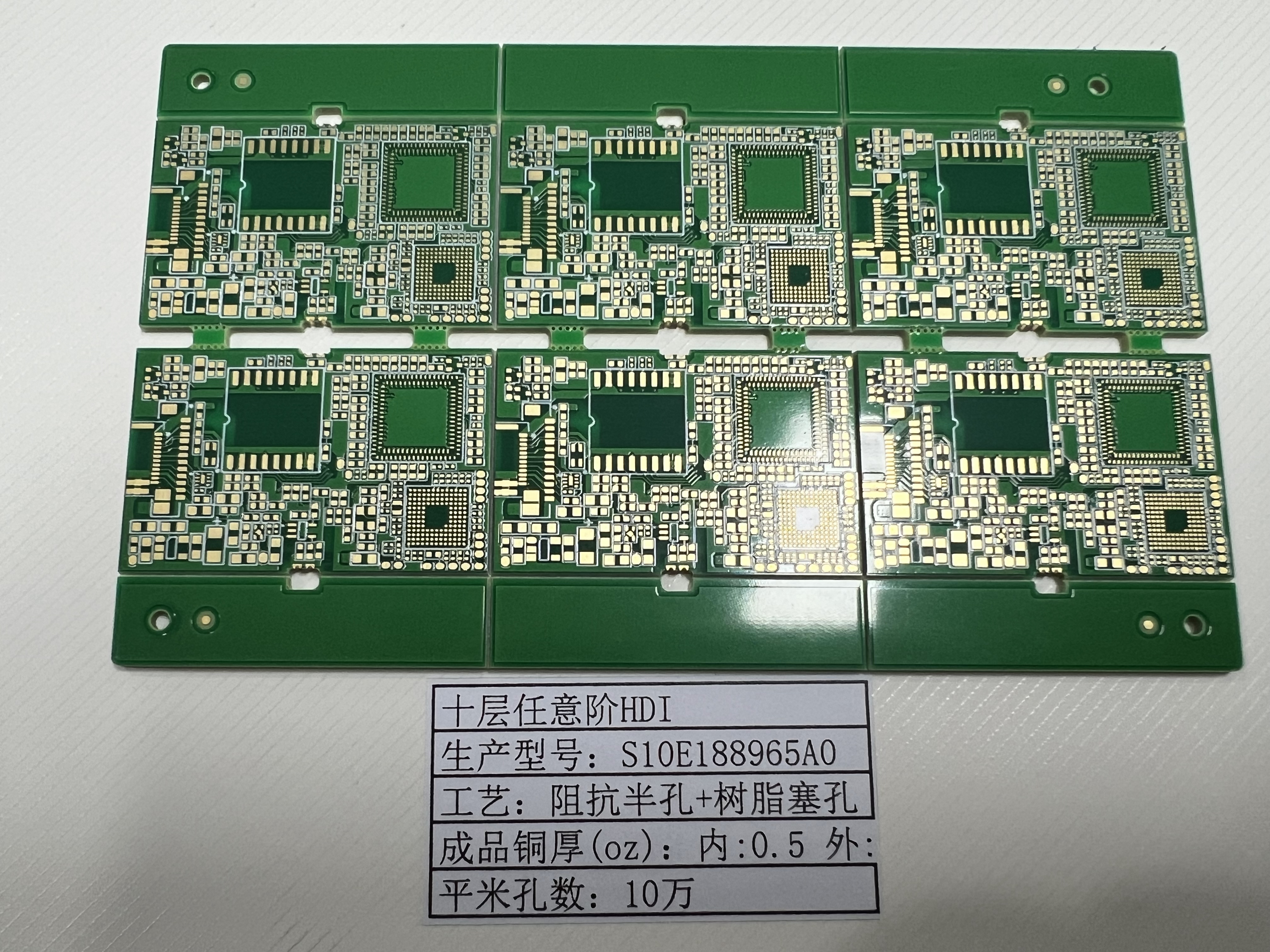
What Are Advanced HDI PCBs and Their Key Characteristics
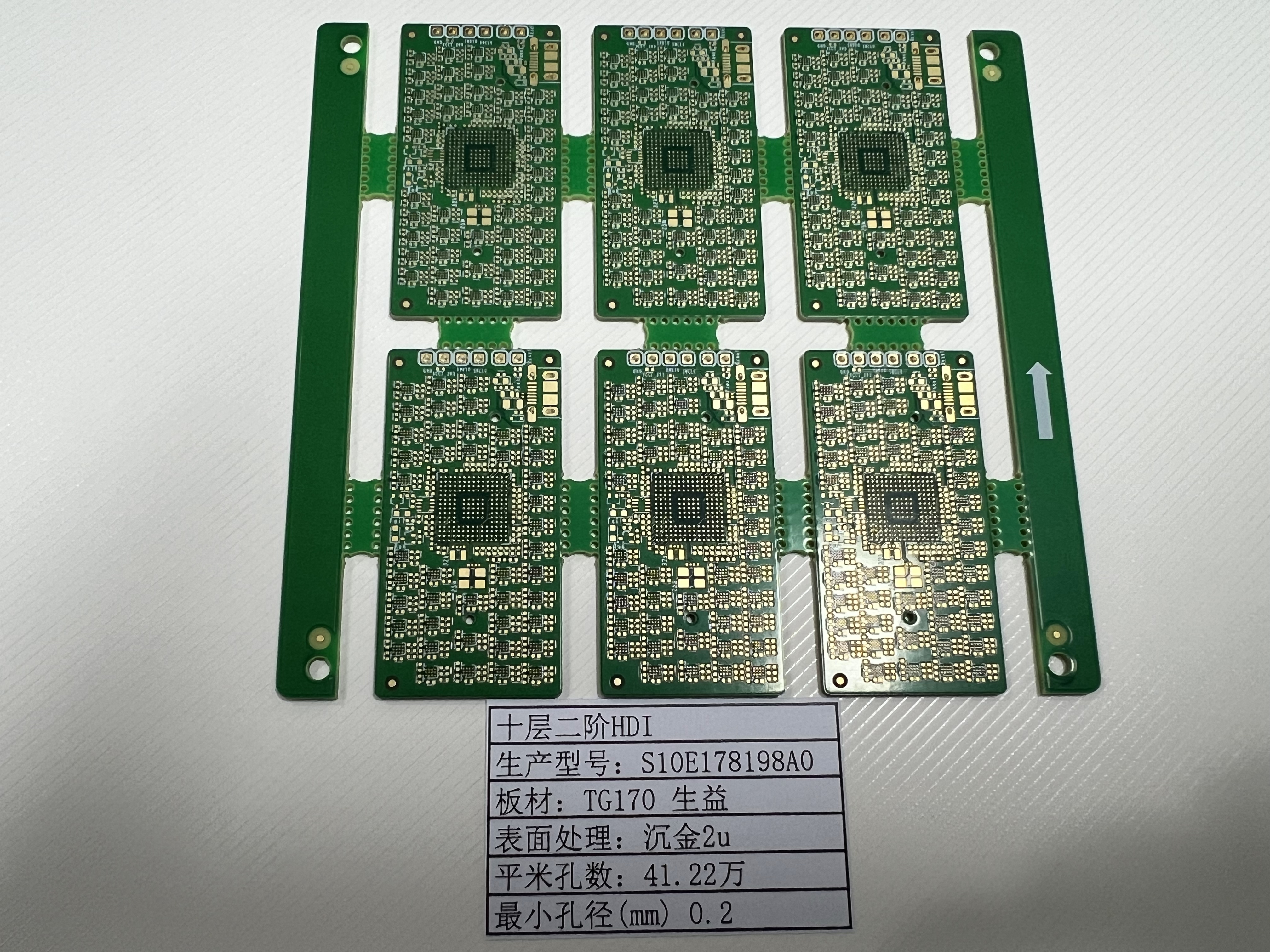
Advanced hdi pcb technology is transforming printed circuit boards by enabling the creation of high-density interconnected PCBs. With advanced hdi pcb solutions, devices can become smaller and more efficient, enhancing overall performance. Over the past decade, advanced hdi pcb technology has become crucial in the electronics industry. LT CIRCUIT stands out as a leading company, offering innovative advanced hdi pcb designs and maintaining a strong focus on producing high-quality products.
Key Takeaways
Advanced HDI PCBs have very small holes made by lasers. They also have thin lines. This helps fit more circuits in a small area. Devices can be smaller, faster, and work better.
These PCBs use special materials and smart designs. This makes signals clearer and more reliable. Devices last longer and work better because of this.
LT CIRCUIT is a leader in HDI PCB ideas. They use new laser tools and careful checks. This gives strong boards that work well for many industries.
Advanced HDI PCB Basics
What Is an Advanced HDI PCB
An advanced hdi pcb uses special technology to fit more parts and connections in a small space. These boards have microvias, which are tiny holes made by lasers. Microvias help connect the different layers of the board. The hdi manufacturing process has steps like laser drilling and laser direct imaging. It also uses sequential lamination. These steps make the board thinner and lighter. They also help the board handle more complex designs.
Advanced hdi pcb boards help engineers make smaller devices. These devices can work faster and use less power. They are used in things like smartphones, medical devices, and high-speed computers. The hdi pcb design uses fine lines, small pads, and many layers. This helps the board have higher density and better performance.
Here is a table that lists the main features of an advanced hdi pcb:
Feature | Description |
|---|---|
Microvia Size | Less than 150 microns, made with laser drilling |
Line Width/Spacing | 3-4 mil (0.076-0.10 mm), allows finer lines |
Pad Size | 0.2 mm to 0.5 mm |
Layer Count | 4 to 50 layers |
Build-up Structure | Multilayer build-up (1+N+1, 2+N+2, etc.) |
Electrical Performance | Improved signal integrity and reliability |
Manufacturing Process | Laser drilling, laser direct imaging, sequential lamination |
Board Thickness | 0.8 to 3.2 mm, with 1.6 mm common |
The hdi manufacturing process uses advanced tools and clean rooms. This helps make sure each board meets strict quality rules. The process helps make small and powerful electronics.
High Density Interconnected PCBs Explained
High-density interconnect, or HDI, means putting more circuits and connections in a small area. A high-density pcb uses microvias, blind vias, and buried vias. These are different from through-hole vias. This lets the board have more layers and better signal paths. The hdi manufacturing process uses thin materials and careful drilling to make these connections.
Here are the main differences between standard printed circuit boards and advanced hdi pcb boards:
Comparison Aspect | Standard PCBs | Advanced HDI PCBs |
|---|---|---|
Layer Count | Up to 50 layers | |
Via Technology | Through-hole vias | Microvias, blind, and buried vias |
Size and Weight | Larger and heavier | Smaller and lighter |
Signal Integrity | Adequate | Superior, better for high-speed signals |
Manufacturing Complexity | Simple | Complex, uses advanced processes |
Design Flexibility | Limited | Greater flexibility for complex layouts |
Electrical Performance | Limited at high frequencies | Better at high frequencies |
A high-density interconnector pcb uses microvias instead of through-hole vias. This change lets engineers fit more paths on the board. It also allows for more complex designs. Engineers use new layer stackups and place microvias carefully. This helps signals move better and reduces interference. The hdi manufacturing process keeps traces and pads close together. This helps make the board smaller and work better.
Some important design rules for high-density interconnect boards are:
Use microvias instead of through-hole vias to add more routing space.
Change layer stackups to bring ground and power planes closer to the top.
Place microvias to make better routing channels.
Keep signal integrity and impedance control as main goals.
Follow IPC standards for reliability and making the boards.
A high-density pcb helps solve problems like signal loss, interference, and heat. The hdi manufacturing process uses special inspection tools. These tools make sure each board works the right way.
LT CIRCUIT’s Role in HDI PCB Innovation
LT CIRCUIT is a leader in hdi pcb innovation. The company uses laser direct imaging (LDI) to make detailed designs. This technology helps make the process faster and more accurate. LT CIRCUIT also uses advanced materials, like metal core PCBs. These materials help with heat and electrical performance.
The company’s hdi manufacturing process does not need photomasks. This saves time and cuts down on waste. LT CIRCUIT cares about the environment. They use fewer chemicals and save energy. Their process works for both small and large orders. This helps them serve many different industries.
LT CIRCUIT’s advanced hdi pcb products are used in electronics, telecom, aerospace, and cars. The company works hard to make high-quality and new products. This makes them a trusted partner for businesses that need high-density interconnect solutions. Their hdi pcb boards meet strict industry rules. They help customers build smaller, faster, and more reliable devices.
Key Features of HDI PCBs
Microvias and Via Technologies
Micro via technology is very important in hdi pcb design. Engineers use microvias to link layers in printed circuit boards. These tiny holes are usually smaller than a strand of hair. They help fit more parts in a small space. This makes electronic devices smaller and lighter. There are different types of microvias. Some are blind microvias, buried microvias, stacked microvias, staggered microvias, skip vias, and Every-Layer Interconnect (ELIC). Blind and buried microvias are used a lot in hdi pcb stackups. Stacked microvias are made by drilling holes right on top of each other. This saves space. Staggered microvias are placed in a step pattern. This makes them stronger in boards with many layers.
Metric | Stacked Microvias | Staggered Microvias |
|---|---|---|
Drilled holes directly on top of each other, connecting multiple layers | Offset via placement on different layers, creating a stepping stone connection | |
Space Efficiency | More space-saving due to direct vertical connection | Takes up slightly more space due to offset placement |
Signal Integrity (2 Layers) | Potentially better due to a shorter electrical path | Good performance |
Reliability (Multilayer) | Lower reliability, especially for 3+ layers, due to drilling and alignment challenges | Higher reliability for multilayer connections due to reduced stress on via walls |
Manufacturability | Requires precise alignment and drilling techniques, increasing cost | Simpler manufacturing process, generally less expensive |
Design Considerations | Ideal for tight designs with minimal via size and potentially better performance for two-layer connections | Suited for designs where space is not a critical constraint but reliability is a major concern, especially for three or more-layer connections |
Micro via technology lets engineers put more pads close together. The hdi manufacturing process uses lasers to make these tiny holes. LT CIRCUIT uses special ways to stack microvias. This helps make strong connections and small board layouts. These methods keep signals clear and help meet the needs of new hdi pcb designs.
Fine Lines and High Layer Count
Fine lines and many layers are important in hdi pcb design. Engineers can make lines as thin as a piece of thread. These lines can be as small as 2 mils wide. This lets them fit more circuits in a small area. It is very useful for high-density pcb jobs.
Parameter | HDI PCB Minimum Value |
|---|---|
Minimum Line Width | 2 mils (0.002 inches) |
Minimum Line Spacing | 2 to 4 mils |
Via Diameter | ≤ 6 mils |
Dielectric Thickness | 1.5 to 4 mils |
Parameter | Inner Layer Minimum | Outer Layer Minimum |
|---|---|---|
Trace Width / Spacing | 2 mil / 2 mil |
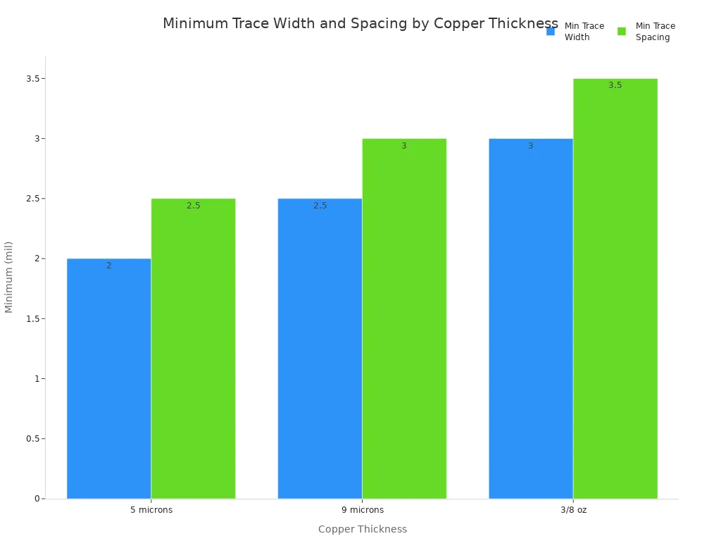
Minimum Trace Width | Minimum Trace Spacing | |
|---|---|---|
5 microns | 2 mil (0.002") | 2.5 mil (0.0025") |
9 microns | 2.5 mil (0.0025") | 3 mil (0.003") |
3/8 oz | 3 mil (0.003") | 3.5 mil (0.0035") |
Adding more layers to hdi pcbs means more connections fit in a thin board. This makes the board thinner and helps it stay strong. Microvias and fine lines help signals travel better and stop them from mixing. Special ways to build the boards, like using lasers and stacking layers, keep everything lined up. These tricks make hdi pcb design good for fast and powerful electronics.
More layers in a thin board make it less thick.
Microvias and fine lines help signals stay strong.
Special building steps keep everything lined up.
More layers make the board harder to build but more useful.
Advanced Materials in HDI PCB Design
Picking the right material is very important in hdi pcb design. Engineers pick materials based on how they handle heat, electricity, and strength. Some common materials are FR-4, polyimide, liquid crystal polymer (LCP), Rogers materials, BT resin, cyanate ester, PTFE, ceramic, and metal-core boards.
Material | Key Properties | Typical Applications and Notes |
|---|---|---|
FR-4 | Cost-effective, good mechanical strength, electrical insulation, higher dielectric constant (Dk) and dissipation factor (Df) | General-purpose PCBs; less suitable for high-frequency HDI due to higher Dk and Df |
Polyimide | High thermal stability (high Tg), chemical resistance, lower Dk and Df than FR-4 | High-temperature and high-frequency applications; aerospace, automotive, medical; more expensive but reliable |
Liquid Crystal Polymer (LCP) | Very low Dk and Df, low moisture absorption, excellent dimensional stability, chemical resistance | High-frequency, millimeter-wave, microwave applications requiring signal integrity |
Rogers Materials | Very low Dk and Df, excellent dimensional stability, good thermal properties | RF and microwave applications; aerospace, defense, telecommunications |
BT Resin | Improved thermal and electrical properties compared to FR-4 | Balanced performance and cost |
Cyanate Ester | Excellent electrical properties and thermal stability | High-performance applications |
PTFE (Teflon) | Exceptional electrical properties at very high frequencies, challenging to process | Specialized high-frequency applications |
Ceramic Substrates | Very high thermal conductivity, smooth high-frequency dispersion | High-temperature environments |
Metal-Core Substrates | High power and high temperature applications | Single or two-layer boards requiring heat dissipation |
Advanced materials help hdi pcbs handle heat and electricity better. Materials that move heat well keep the board cool. Materials with low dielectric constant help signals stay clear. LT CIRCUIT picks strong materials to make sure their hdi pcbs last long and work well.
Microvias under pads help make tiny layouts and move heat away.
Lasers make very small microvias for tight spaces.
Picking materials with high glass transition temperature (Tg) and good heat flow keeps boards strong.
LT CIRCUIT Quality Standards
LT CIRCUIT follows strict rules to make sure every hdi pcb is high quality. The company has ISO 9001:2015 and IATF 16949:2016 certificates. These show they care about quality. LT CIRCUIT also meets UL safety rules for the US and Canada.
LT CIRCUIT uses Laser Direct Imaging (LDI) for sharp circuit patterns.
Lasers drill microvias as small as 0.10 mm. CNC drills make some bigger holes for better strength.
Electroplating uses sound waves and special acid to cover holes evenly.
The company checks every board with Automated Optical Inspection (AOI). They also check the process often. They watch microvia size, pad size, plating, and depth. LT CIRCUIT follows IPC rules for microvia design and stacking. They use copper layers to make microvias with no gaps. They test boards with Interconnect Stress Testing (IST) and D coupon analysis to make sure they are strong.
LT CIRCUIT’s focus on quality, good materials, and careful micro via work means their hdi pcb design meets top industry rules. Customers trust LT CIRCUIT for strong, high performance boards for tough jobs.
Advantages and Applications
Miniaturization and Signal Integrity
HDI PCBs help make parts much smaller. Engineers use hdi pcb design to put small parts close together. Microvias and thin lines let more circuits fit in less space. This makes things like smartphones, tablets, and wearables smaller and lighter.
Devices get smaller because HDI PCBs need fewer boards.
Engineers can put passive parts inside the board to save space.
Flexible and rigid-flex HDI PCBs help make bendable devices for wearables and medical tools.
HDI pcb design also keeps signals strong and clear. Engineers use special layers and careful routing. Microvias and blind vias help signals move fast and stay clear. These features help modern devices send signals quickly and work better.
Reliability and Cost-Effectiveness
HDI pcbs are very reliable. Good materials and careful building lower the chance of problems. For example, HDI PCBs can have failure rates as low as 0.1% in hard places.
Strong materials and careful drilling stop cracks and damage.
Careful testing checks quality and makes boards work better.
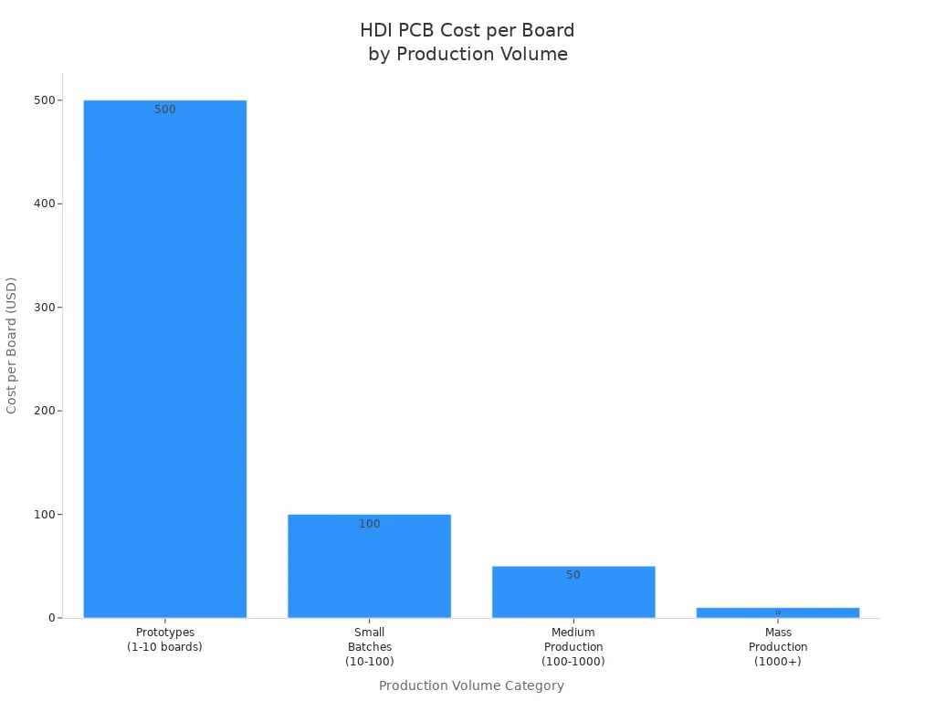
HDI PCBs also save money when making many boards.
Smaller boards cost less to ship and store.
Making many boards at once spreads out costs, so each board is cheaper.
Smart designs help cut down on waste.
Where HDI PCBs Are Used
Many industries use HDI PCBs for small size and good performance.
Consumer electronics: smartphones, tablets, and wearables
Automotive: electric cars and smart driving systems
Healthcare: medical tools and portable monitors
Telecommunications: fast network equipment
Industrial: automation and smart factories
Aerospace and defense: strong, small electronics
LT CIRCUIT Solutions for Industry
LT CIRCUIT gives quality HDI PCB solutions for many areas. In cars, they use strong materials and careful connections for safety and good work. For medical tools, LT CIRCUIT makes sure there is 99.9% precision, helping companies get products ready faster. Their focus on quality and reliability helps industries that need better performance and trust.
Advanced HDI PCBs are very important in today’s electronics.
They help fit more circuits in a small space.
They let engineers add more features to tiny gadgets.
LT CIRCUIT uses special lasers to drill tiny holes and checks every board carefully.
Their HDI PCBs are made to work well and last a long time.
Companies that want strong and high-quality HDI PCBs can count on LT CIRCUIT’s skills.
FAQ
What makes HDI PCBs different from standard PCBs?
HDI PCBs use microvias and fine lines. These features allow more circuits in less space. Devices become smaller and work faster.
Why do engineers choose LT CIRCUIT for HDI PCB solutions?
LT CIRCUIT uses advanced tools and strict quality checks. Customers trust their reliable products for many industries.
Can HDI PCBs improve device performance?
Yes! HDI PCBs help signals stay clear and strong. Devices run faster and last longer with these boards.
See Also
Explore Cutting-Edge Methods For HDI PCB Prototyping
Essential Design Tips For Reliable HDI PCB Production
The Process Behind Designing And Making Any Layer HDI PCBs
Innovative HDI Rigid-Flex PCBs Combining Strength And Size
Evaluating Costs And Benefits Of Advanced HDI Microvia Designs