Discover Advanced HDI PCB Prototype Techniques Today
The fast progress in HDI PCB prototype development utilizes new methods. These include laser drilling and creating tiny holes known as microvias. These advancements help build smaller, lighter, and more efficient circuit boards. For example:
HDI PCB prototype technology allows for smaller PCBs that can accommodate more components.
Laser drilling enables the creation of deep microvias for compact designs.
This progress aligns with the demand for tiny gadgets, ensuring that devices operate effectively and have a longer lifespan.
Key Takeaways
HDI PCBs help make smaller and better designs for devices like phones and smartwatches.
Laser drilling makes tiny holes for strong connections in tight spaces, improving how circuits work.
Testing prototypes helps find problems early, saving money and time while making better products.
Machines like AOI systems check for mistakes fast, keeping production consistent and reliable.
Picking good materials and simpler designs lowers costs and makes HDI PCBs work better.
HDI PCB Prototype: Overview and Importance
Key Features of HDI PCBs
HDI PCBs are special because they support dense designs. They have features like:
Microvias: Very small holes, under 150 microns wide, for tight connections.
Blind Vias: These link outer layers to inner ones without going through the board.
Buried Vias: These only connect inner layers, keeping the surface simple.
Feature | Description | Benefits |
|---|---|---|
Microvias | Tiny holes, less than 150 microns wide. | Helps make compact and space-saving designs. |
Finer Line Widths | Lines as thin as 3 mil (0.075 mm). | Allows for more detailed circuit layouts. |
Higher Layer Counts | Can fit 20+ layers in the same thickness. | Supports more parts and complex circuits. |
Advanced Manufacturing Processes | Uses laser drilling and layered assembly. | Makes high-density connections possible. |
These features are key for modern gadgets where space and performance matter most.
Applications in Modern Electronics
HDI PCBs are important for many industries. They handle complex designs in small spaces, making them perfect for:
Smartphones and tablets
Wearable tech like smartwatches and fitness bands
Car electronics, like safety systems and entertainment
Aerospace and defense equipment
Medical tools like implants and testing devices
High-speed computers
Advanced industrial machines
In today’s tech world, HDI PCBs help make devices smaller and better. They improve signals and meet the needs of modern users.
Why Prototyping Matters for HDI PCBs
Prototyping is a key step when making HDI PCBs. It helps check if the design works as planned. Engineers can spot problems early and fix them. This lowers mistakes in the final product and makes production easier. Prototypes also test how the board works in real life, ensuring it’s reliable and high-quality.
Prototyping saves time and money by reducing risks. It’s a must for successful HDI PCB designs.
Advanced Technologies in HDI PCB Prototype Manufacturing
Laser Drilling for Microvias
Laser drilling has changed how microvias are made in HDI PCBs. This method uses lasers to drill tiny holes with great accuracy. Modern lasers can make holes smaller than 100 microns wide. They are also very fast, drilling up to 4,500 holes each second.
Improvement Aspect | Measurement/Value |
|---|---|
Throughput with 2-head CO2 laser | 1,500 holes per second |
Throughput with advanced laser | |
Position accuracy | Less than +/-10 μm |
Diameter of through-holes | <100 μm |
This process is key for making reliable connections in tight spaces. It helps create high-performing circuits for advanced electronics.
Sequential Lamination Process
Sequential lamination is important for building HDI PCBs. It involves adding and bonding layers one at a time. Limiting the process to two or three cycles saves money and improves reliability.
Benefit | Description |
|---|---|
Cost Reduction | |
Signal Integrity | Fewer cycles help keep signals clear and strong. |
Increased Reliability | Reducing cycles makes the final product more dependable. |
This method also keeps signals stable, which is needed for fast and advanced devices. Sequential lamination ensures HDI PCBs meet modern tech needs.
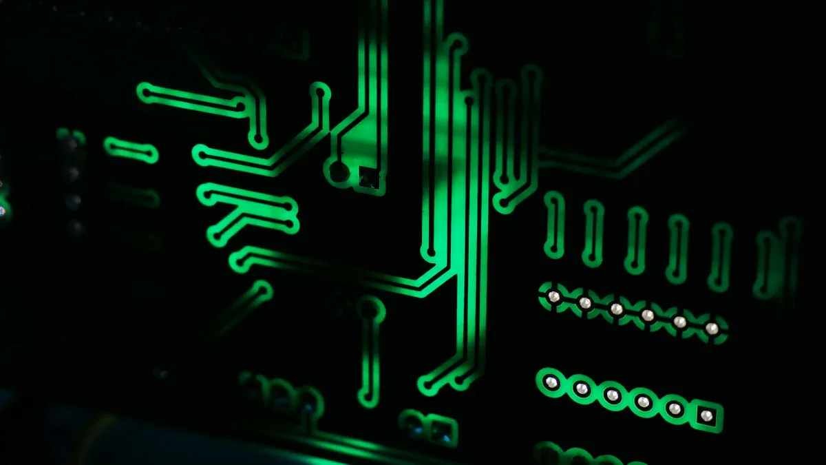
High-Precision Etching Techniques
High-precision etching helps create detailed circuit patterns on HDI PCBs. It uses special tools to make very fine lines and spaces. Direct imaging systems allow for better details, while plasma etching cleans up vias. Additive processes make designs even more accurate and compact.
These techniques improve the quality of circuits and make devices smaller. High-precision etching ensures HDI PCBs work well and last longer.
Automated Optical Inspection Systems
Automated Optical Inspection (AOI) systems are vital for checking HDI PCBs. They use special cameras and software to find problems. AOI helps spot issues early, saving time and money in production.
How AOI Works
AOI systems scan PCBs with high-quality cameras. They compare the scan to a design file. If something doesn’t match, it gets flagged for review. This ensures the board matches the original plan perfectly.
Tip: AOI systems are great at finding misaligned parts, broken lines, and solder mistakes.
Benefits of AOI Systems
Using AOI in HDI PCB prototyping has many benefits:
Accuracy: Finds even tiny problems for better-quality boards.
Speed: Inspections are fast, avoiding production delays.
Cost Savings: Early fixes prevent expensive rework or waste.
Consistency: Keeps all prototypes at the same high standard.
Feature | Benefit |
|---|---|
High-resolution cameras | Spots small defects accurately. |
Automated process | Makes inspections faster and reduces mistakes. |
Real-time feedback | Fixes can be made right away. |
Why AOI Matters for HDI PCBs
HDI PCBs are complex with small parts and thin lines. Manual checks might miss important problems. AOI systems handle this complexity easily. They ensure prototypes are reliable and perform well.
Using AOI technology helps you make perfect HDI PCBs. It’s a smart way to stay ahead in today’s tech world.
Step-by-Step HDI PCB Prototype Manufacturing Process
Design and Layout Preparation
The first step is to plan the design and layout. This ensures the board meets all technical needs. Follow these simple design tips:
Use small trace widths and spacing for proper fabrication.
Check via and pad ring sizes for accuracy.
Know the right drill sizes for microvias.
Keep copper edges clear to avoid short circuits.
Set solder mask openings to stop solder bridges.
Space traces apart to reduce signal interference.
Mark areas where no traces or vias should go.
Work with your PCB maker early to match their abilities.
Tip: Keep your design simple. It saves time, cuts costs, and boosts reliability.
Material Selection and Layering
Picking the right materials is key for a strong HDI PCB. Good materials help the board handle modern tech demands. Look for these qualities:
Glass transition temperature (Tg): At least 180°C for heat stability.
Dielectric constant (Dk): Below 5 for better signal performance.
Coefficient of thermal expansion (CTE): Under 70 ppm to avoid warping.
Loss tangent (tanδ): Between 0.01 and 0.002 to limit signal loss.
Top materials include Isola-370 HR for heat resistance and Rogers 4000 series for high-frequency use. For networking, Panasonic Megtron 6 is very reliable.
Note: Choose materials based on your device’s needs, like speed or heat resistance.
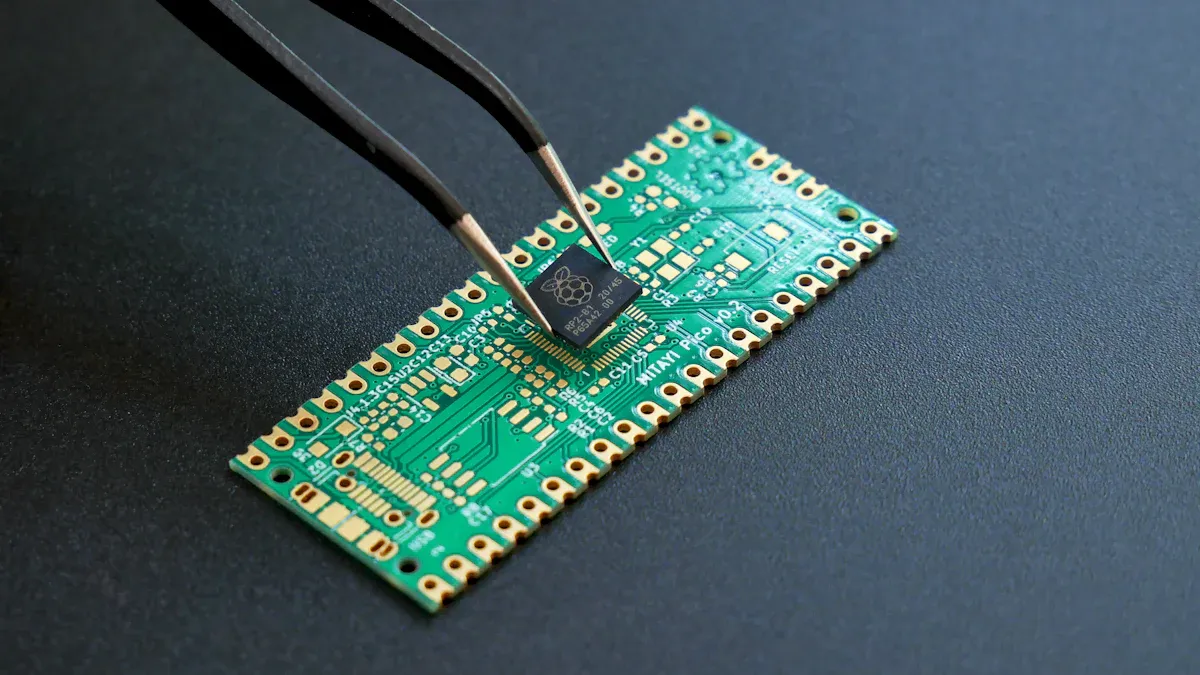
Microvia Formation and Laser Drilling
Microvias are tiny holes needed for compact HDI PCBs. Laser drilling is the best way to make them. CO2 lasers drill microvias as small as 50 μm wide. This method is very precise, with an accuracy of +/-10 μm. It keeps circuits working well.
Modern lasers can drill up to 4,500 holes per second. This makes the process fast and efficient. Even complex designs can be made quickly and reliably.
Tip: Use laser drilling for accurate and defect-free microvias.
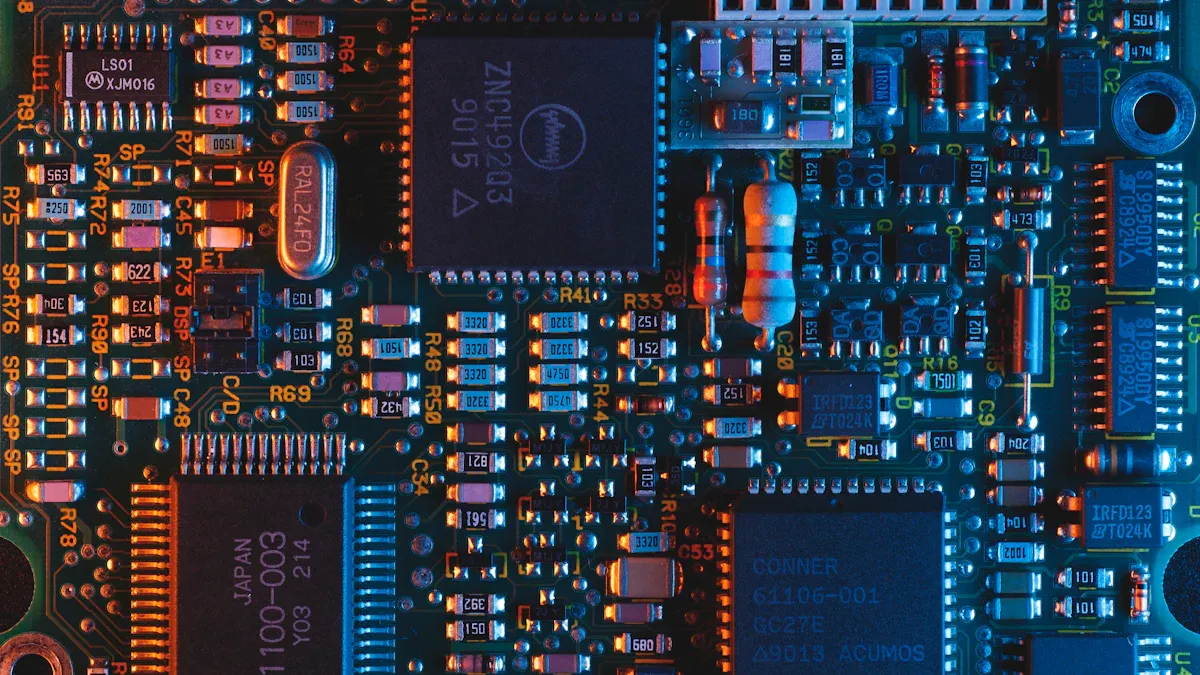
Copper Plating and Circuit Etching
Copper plating is very important in making HDI PCBs. It helps create strong and reliable connections between layers. In this step, a thin copper layer is added to microvias and paths. Electroplating is used, where electricity spreads copper evenly on the board. This makes a surface that carries fast signals well.
Next, circuit etching shapes the paths for electrical signals. Chemicals remove extra copper, leaving only the needed patterns. Precise etching ensures clean and accurate lines. This step is key for keeping your HDI PCB working well, especially in devices needing strong signal quality.
Tip: Make sure the copper layer is thick enough. This avoids problems like signal loss or overheating.
Final Assembly and Quality Testing
The last step is putting all parts together. Chips, resistors, and capacitors are placed on the PCB using SMT. This method saves space and makes the board stronger. After assembly, the board is tested to ensure it works properly.
Testing checks how well the HDI PCB performs. Stress tests mimic long-term use, while HALT and HASS find weak spots. Fire safety tests, like those by NEMA and NFPA, confirm the board meets safety rules.
Quality Check Step | What It Does |
|---|---|
Material Check | Makes sure laminates and copper meet the needed standards. |
Finds problems in PCB layers early in the process. | |
X-Ray Check | Confirms vias and through-holes are connected properly. |
Other tests include vibration, heat changes, and weather exposure. These ensure the PCB can handle real-world conditions. Electrical tests make sure the board supports fast signals without breaking.
Note: Full testing ensures your HDI PCB is safe and works perfectly.
Benefits of Advanced Techniques in HDI PCB Prototyping
Better Performance and Dependability
New HDI PCB techniques make electronics work better and last longer. These methods allow for detailed designs in small spaces. They reduce signal problems and improve signal strength. Devices like phones and smartwatches benefit from shorter signal paths. This lowers signal mix-ups and interference, making data transfer faster and more reliable.
Smaller trace lines improve signal flow and quality.
Laser drilling creates strong and lasting connections.
Prototyping Technique | Description | Reliability Improvement Metrics |
|---|---|---|
Rapid Prototyping | Quickly builds models for testing and fixes issues fast. | Cuts time to find and fix design problems. |
Digital Prototyping | Tests designs in virtual settings before making real models. | Ensures designs meet exact needs. |
Incremental Prototyping | Tests small parts step-by-step for better results. |
These methods make HDI PCBs essential for high-tech devices.
Smaller Size and Better Space Use
Modern gadgets need to be small, light, and efficient. HDI PCB prototyping helps by shrinking and organizing designs. Techniques like MIC make even complex boards fit into tiny devices.
Smaller boards make products more compact.
More parts fit into less space for better use.
Lighter boards make gadgets easier to carry.
HDI PCBs are key for small devices like wearables, medical tools, and 5G gadgets. They save space while keeping devices powerful and effective.
Quicker Manufacturing Times
Advanced methods speed up how HDI PCBs are made. Tools like laser drilling, AOI, and lamination make production faster without losing quality. Rapid prototyping helps test and improve designs quickly, getting products ready sooner.
Tip: Faster production keeps you ahead in the tech world.
These techniques save time and cut costs by reducing mistakes. With shorter timelines, you can meet deadlines and deliver advanced products faster.
Better Signal Quality and Heat Control
Keeping signals clear and managing heat are very important for HDI PCBs, especially in powerful devices. New methods in HDI PCB prototyping help designs keep strong signals and handle heat well, even in small spaces.
Ways to Improve Signal Quality
HDI PCBs make signals better by shortening their paths. Shorter paths mean signals move faster and with less trouble. Using special techniques like pairing signal lines and adding ground layers also helps. These steps stop signals from mixing up or causing problems, making them work better in fast devices.
Improvement Type | Description |
|---|---|
Signal Quality | |
Stops signals from mixing | |
Reduces signal problems | |
Adds ground layers for better flow | |
Pairs signal lines for accuracy |
Tip: Remove extra parts in vias to avoid signal issues. This keeps signals clear and strong.
Heat Control Methods
Good heat control stops HDI PCBs from getting too hot. Tiny holes called thermal vias help move heat away from parts. Using materials that spread heat well also keeps the board cool. These features make sure the board stays safe, even when working hard.
Improvement Type | Description |
|---|---|
Heat Control | Uses thermal vias to move heat |
Keeps parts cool in tight spaces | |
Uses heat-friendly materials |
By using these smart methods, you can make HDI PCBs that handle both signals and heat well. This helps devices work better and last longer, even in tough conditions.
Note: Managing heat properly makes your HDI PCB last longer and work without problems.
Challenges and Solutions in HDI PCB Prototype Manufacturing
Managing High Manufacturing Costs
Making HDI PCBs costs a lot because of special materials. These include pricey laminates and prepregs needed for advanced designs. Methods like laser drilling and adding layers also raise costs. Tight tolerances in prototypes can lower success rates, especially at first. Testing takes more time and adds to expenses.
Challenge Type | Description |
|---|---|
Materials | Special laminates and prepregs are expensive. |
Manufacturing processes | Laser drilling and layer stacking cost more. |
Yield | Tight tolerances reduce success rates early on. |
Testing | Complex testing takes extra time and money. |
To save money, design boards to use fewer materials. Simplify steps to make production faster. Work with skilled manufacturers to find ways to cut costs without losing quality.
Addressing Design Complexity
HDI PCB designs are tricky because they have many layers and tiny holes. These details make production harder and more expensive. For example, more microvias need extra time and effort. Adding layers also increases the number of steps to build the board.
Evidence Description | Impact on Cost and Feasibility |
|---|---|
More microvias mean more time and effort to produce. | Raises costs due to extra labor and precision needed. |
Extra layers add more steps to the process. | Increases production time and expense. |
Simplifying designs can reduce these challenges. | Saves money and makes production easier without losing quality. |
To handle this, keep designs simple. Use fewer layers and place microvias wisely. This lowers costs and makes boards easier to produce.
Ensuring Quality and Consistency
Keeping HDI PCBs high-quality needs close checks during production. Important factors like soldering heat and chemical etching must be watched. Automated systems help find mistakes early, ensuring every board meets top standards.
Watch soldering heat levels to avoid problems.
Track chemical etching rates to keep designs accurate.
Use automated checks after assembly to spot defects fast.
These steps ensure your HDI PCBs are reliable and meet modern tech needs.
Overcoming Material Limitations
Material limits can cause problems in making HDI PCBs. Picking the wrong materials might lead to signal issues, overheating, or breaking. To avoid these, you need smart strategies.
One way is to choose the best materials. Options like FR4, polyimide, and ceramics are great. They handle heat, stay strong, and support fast signals. For instance, polyimide is good for flexible circuits, while ceramics work well in high-frequency devices.
A clear layout design is also important. Placing parts and paths carefully reduces mistakes. This makes the board more reliable and works better. Design software can help by testing signals and improving the layout before production.
Working with engineers early can solve material problems. Their advice finds issues before they happen, saving time and money. Following Design for Manufacture (DFM) rules also helps. It matches your design with factory abilities, making production smoother.
Strategy | Description |
|---|---|
Choice of Material | Use materials like FR4, polyimide, and ceramics for strength and performance. |
Optimum Layout Design | Careful part placement avoids errors and boosts reliability. |
Advanced Software Tools | Design tools test and improve layouts before production. |
Interdisciplinary Cooperation | Engineers help spot and fix problems early. |
DFM Compliance | Follow DFM rules to make production easier and better. |
Using these ideas, you can solve material challenges. This ensures your HDI PCBs are strong, efficient, and ready for modern tech needs.
New methods like laser drilling and sequential lamination have changed HDI PCB prototyping. These techniques help make small, powerful prototypes for today’s electronics. Using them ensures dependable results and keeps you competitive in technology. Try these advanced methods now to fully improve HDI PCB prototyping.
FAQ
What makes HDI PCBs special compared to regular PCBs?
HDI PCBs have tiny holes, thinner lines, and more layers. These features help make smaller designs that work better. They also use advanced methods like microvias and layer-by-layer building, perfect for today’s gadgets.
Why is laser drilling useful for HDI PCBs?
Laser drilling makes tiny, accurate holes called microvias. These holes are key for small, high-density designs. This method ensures strong connections between layers, making HDI PCBs more reliable and efficient.
How can you lower costs when making HDI PCBs?
You can cut costs by using fewer layers and microvias. Working with skilled manufacturers can also improve production steps. Picking affordable materials that still work well is another way to save money.
What materials are best for HDI PCBs?
Materials like FR4, polyimide, and ceramics work great. They handle heat, last long, and support fast signals. Choose materials based on what your device needs, like flexibility or heat resistance.
How do automated optical inspection (AOI) systems help with quality?
AOI systems find mistakes early during production. They use cameras to check if the PCB matches the design. This reduces errors, improves accuracy, and keeps all prototypes high-quality.