Aerospace PCB Manufacturing stringent requirements in 2026

In 2026, aerospace pcb manufacturing demands absolute precision. Failure is not an option when a single defect can ground a fleet or silence a satellite. You must meet AS9100 quality systems, IPC Class 3 fabrication, and survive brutal extremes from -55°C to +125°C plus relentless vibration. These stringent standards and requirements separate commercial boards from flight-critical hardware. Aerospace pcb assembly leaves no room for error, and mission-critical reliability depends on every layer, via, and joint. What specific materials, processes, and reliability requirements must you master to guarantee compliance? This post gives you a clear roadmap. You will learn how to navigate these critical demands and achieve the reliability your programs demand.
Key Takeaways
Aerospace PCBs must work perfectly in extreme temperatures and vibration, unlike commercial boards.
You must follow AS9100D, IPC Class 3, and other standards to ensure reliability and safety.
Choose materials like high-Tg FR-4 or polyimide that survive -55°C to +125°C and vibration.
Design with controlled aspect ratios, annular rings, and thermal vias to prevent failures.
Assembly requires cleanliness, selective soldering, and full traceability for zero defects.
Test every board with flying probe, X-ray, thermal cycling, and vibration to prove reliability.
Select a manufacturing partner with aerospace experience, certifications, and in-house capabilities.
These practices protect lives and missions, turning compliance into confidence.
Aerospace PCB Manufacturing: The 2026 Landscape
Why Failure Is Not an Option
Mission-Critical Reliability in Extreme Environments
Aerospace PCBs differ fundamentally from commercial boards. Commercial electronics tolerate a small percentage of field defects, with defect rates reaching 3–5%. Aerospace PCBs demand effectively 100% reliability. No field defects are acceptable. Your board must operate in space, at high altitude, and in defense platforms where repair access does not exist.
Dimension | Commercial PCBs | Aerospace PCBs |
|---|---|---|
Reliability | Tolerate 3–5% field defects | Effectively 100% reliability required |
Temperature range | Standard FR-4 with Tg 130°C–150°C | -55°C to +125°C; high-Tg FR-4 above 170°C or polyimide |
Vibration tolerance | Not designed for sustained flight vibration | Must withstand launch and flight vibration profiles |
Service life | 3–5 years typical | Decade or more without field repair access |
The "tough triangle" of requirements governs every decision. You must satisfy AS9100 quality management, IPC Class 3 fabrication, and survival under radiation, vibration, and thermal cycling. These three pillars form the foundation of aerospace pcb manufacturing.
The Cost of Failure: Safety and Financial Risks
A failed board can ground a fleet or silence a satellite. The financial stakes extend far beyond the board itself. Recalls, mission delays, and lost contracts follow any field failure. Safety risks to crew and passengers make reliability requirements non-negotiable.
Testing is the final, non-negotiable step in aerospace PCB design. Before deployment, boards must undergo extensive environmental testing to simulate the extreme conditions they'll face. Thermal cycling tests, for instance, expose the PCB to rapid temperature changes between -55°C and 125°C to check for material expansion or solder joint failure. Vibration tests replicate launch conditions, while radiation testing ensures functionality in space.
Key Drivers for 2026
High-Frequency and High-Speed Applications
Modern aerospace systems span avionics to propulsion control. These systems demand PCBs that handle high-speed data transmission, power management, and miniaturization. The adoption of 5G technology in aerospace communications is transforming satellite systems, UAVs, and aircraft. High-frequency PCBs are essential for efficient 5G-based operations. As aerospace companies invest in next-generation communication technologies, demand for specialized PCBs capable of handling high-frequency signals continues to rise.
Miniaturization and Increased Layer Counts
Miniaturization is a major trend driven by the need for smaller, lighter, and more powerful components in avionics, satellites, and drones. This creates opportunities for PCB manufacturers to develop smaller, more efficient designs with improved performance. Multi-layer and flexible PCBs enable the integration of these high-performance systems. You must balance reduced size against functionality and thermal management.
Evolving Regulatory Landscapes
Export controls like ITAR shape every aerospace pcb assembly decision. Compliance with ITAR registration, RoHS, and REACH adds layers of documentation and material verification. Your certification path must account for these evolving rules. Environmental requirements for material sourcing and disposal grow stricter each year. A manufacturing partner who tracks these changes protects your program from costly delays.
2026 Standards & Certifications
AS9100D and NADCAP Accreditation
Understanding AS9100 Rev D
AS9100 Rev D forms the foundation of aerospace pcb manufacturing quality. This standard builds on ISO 9001:2015 and adds aerospace-specific demands. Certification to AS9100D proves your manufacturer can meet top-tier quality, safety, and reliability standards for mission-critical applications. The standard enforces strict documentation, traceability, and process control. These controls minimize defects and boost product reliability. AS9100 aerospace compliance also aligns with FAA, DoD, and NASA rules. This alignment matters for government contracts. The standard supports risk management through proactive assessment and corrective actions. Supply chain credibility follows, because most aerospace OEMs and Tier 1 suppliers require AS9100 certification from approved vendors. AS9100D includes ISO 9001 by default. A certified manufacturer therefore meets general industry standards and exceeds them with aerospace-specific requirements.
The Role of NADCAP in Special Processes
Nadcap accreditation covers specific special processes, such as coatings, chemical processing, heat treating, welding, and non-destructive testing. The program depends on an AS9100-based quality system. A supplier must hold AS9100 certification before Nadcap auditing can begin. The audit process follows a defined sequence. The OEM asks the supplier to apply for Nadcap certification. The supplier contacts Nadcap and requests an auditor through the Performance Review Institute (PRI). The supplier then confirms that relevant special processes meet Nadcap requirements. Nadcap schedules the audit and assigns an auditor. The auditor presents findings and highlights non-conformances. The supplier and PRI technical staff review the report. All non-conformances must be resolved before the report reaches the prime subscriber. A task force at the OEM confirms the findings. The supplier resolves any remaining issues and receives a certificate.
Aspect | AS9100 Revision D | Nadcap Accreditation |
|---|---|---|
Nature | A standard defining requirements for an aerospace quality management system (QMS), aligned with ISO 9001:2015 | An accreditation program for aerospace-related companies, auditing specific special processes |
Scope | Applicable to any aerospace company implementing a QMS | Limited to companies performing specific special processes |
Role in special process approval | Provides the foundational QMS requirements a supplier must have in place | Confirms a supplier meets all requirements for a specific special process |
Relationship | Prerequisite for Nadcap | Depends on an AS9100-based QMS being established first |
IPC Class 3 Requirements and Beyond
IPC-6012 Class 3: High Reliability
IPC Class 3 requirements define high-reliability workmanship and acceptance expectations. These rules apply where failure can create serious performance or safety risks. IPC-6012 and IPC-A-610 serve as the common standards for rigid board qualification, fabrication quality, and assembly acceptance. IPC Class 3 reliability standards push tolerances tighter than Class 2. Plating thickness, annular ring, and hole quality all face stricter limits. Your fabricator must prove process control, not just final inspection.
IPC-6012DA: Aerospace Addendum
The space and military avionics addendum, IPC-6012DA, extends Class 3 for aerospace. It adds rules for thermal cycling, outgassing, and microvia reliability. These additions reflect the extreme environments that aerospace PCBs face. The addendum also tightens acceptance criteria for voids and copper wrap. Compliance with this addendum separates flight-ready hardware from general high-reliability boards.
Military and Compliance Standards
MIL-PRF-31032 for Military Electronics
MIL-PRF-31032 is a performance specification titled "Printed Circuit Board/Printed Wiring Board, General Specification For." Its scope establishes general performance requirements for PCBs and PWBs and the verification requirements for ensuring that these items meet the applicable performance requirements. It is mandatory for military and DoD production. Every PCB produced for military use must come from a company certified to the specification, with no exceptions. The specification covers rigid, flex, and rigid-flex boards under one QML umbrella. It defines material and process verification, reliability testing, traceability, and performance-based compliance. Electrical test limits include continuity below 10 Ω, isolation above 2 mΩ, and voltage of at least 40 volts unless otherwise specified. Group A testing follows a C=0 sampling plan on thermally stressed cross-sections of every panel in X and Y directions. Tests cover solderability, ionic contamination, dimensional and hole sizes, plating adhesion, solder mask adhesion, legend adhesion, surface finish thickness by XRF, bow and twist, electrical testing, and copper tensile and elongation. Military-grade documents include a certificate of conformance, IPC J-STD-001E, material specifications, calibrated tool records, reflow profiles, AOI reports, flying probe reports, as9102 first article inspection reports, and ionic cleanliness reports.
ITAR, RoHS, and REACH Compliance
ITAR registration governs defense-related PCB work. You must verify that your manufacturer holds the proper registration before sharing controlled technical data. RoHS and REACH compliance add material restrictions and documentation duties. These rules affect solder alloys, surface finishes, and laminate chemistry. A partner who tracks these evolving rules protects your program from delays and penalties.
Material Selection for Mission Success
Your material choices decide whether a board survives -55°C to +125°C, launch vibration, and years without repair. Every laminate, copper foil, and finish must earn its place.
Choosing the Right Base Materials
High-Tg and Low-CTE FR-4
Standard FR-4 with a glass transition temperature (Tg) of 130°C–150°C cannot carry flight hardware. You need high-Tg FR-4 above 170°C at minimum. The coefficient of thermal expansion (CTE) matters just as much. Choose laminates with controlled, low Z-axis CTE for any large multilayer board or wide temperature swing.
Polyimides and PTFE for High-Frequency
Polyimide and PTFE serve different missions. Compare their key properties:
Property | PTFE Laminate | Polyimide Laminate |
|---|---|---|
Dielectric Constant (Dk) | 2.5–10.2 | 2.8–4.1 |
Dissipation Factor (Df) @ 10 GHz | 0.0014–0.0038 | 0.003–0.01 |
Glass Transition Temp (Tg) | >200°C | >250°C |
High-Frequency Suitability | Excellent — RF, microwave, satellite | Moderate — flexible high-frequency circuits |
PTFE's low Dk supports faster signal propagation and stable impedance control. Its very low Df minimizes attenuation at high frequencies, which makes it the preferred choice for satellite communication systems. Polyimide offers balanced electrical properties with mechanical flexibility, and its thermal stability suits avionics. Polyimide's CTE of 20–40 ppm/°C runs higher than FR-4, so you must handle it carefully during manufacturing. PTFE requires specialized lamination techniques to prevent creep, which would otherwise degrade dimensional stability and signal integrity.
Conductor and Surface Finish Considerations
Rolled Annealed Copper for Flexibility
Use rolled annealed copper instead of electrodeposited copper. The annealing process relieves internal stresses in the traces and reduces cracking risk. For flex PCBs, copper thickness between 0.25 oz (9 µm) and 2 oz (70 µm) balances flexibility against durability. Design traces with rounded corners and smooth transitions to minimize stress concentrations. Add stiffeners such as FR4, polyimide, or polyester at connector and component areas to reduce mechanical stress.
ENIG, ENEPIG, and Immersion Silver
Your finish choice drives solder joint reliability. Review the trade-offs:
Attribute | ENIG | ENEPIG | Immersion Silver |
|---|---|---|---|
Black pad risk | Present | Eliminated | No nickel barrier |
Shelf life | 12+ months | 12+ months | 6–12 months |
Multiple reflow | 3–5 cycles | 5+ cycles | Degrades faster |
High-frequency performance | Nickel losses above 1 GHz | Same RF concerns as ENIG | Best — highest conductivity |
Wire bonding | Aluminum wire only | Gold, aluminum, copper | Not suitable |
ENIG delivers exceptional flatness for BGA and fine-pitch parts at 0.5 mm or below, with nickel at 3.05–5.08 µm and gold at 0.025–0.76 µm. Its black pad defect remains the main risk. ENEPIG adds a palladium layer of 0.025–0.2 µm, eliminates black pad, and supports universal wire bonding. Immersion silver wins on RF and high-speed digital boards above 5 GHz, though it tarnishes in humid conditions. ENEPIG withstands temperatures up to 150°C and prevents oxidation while improving solderability.
Solder Mask and Silkscreen
High-Reliability Solder Masks
Solder masks must hold up under thermal cycling and vibration. Select masks qualified to IPC Class 3 standards, with strong adhesion and resistance to flux and cleaning chemicals. Adhesion failures show up as lifted mask after thermal stress, so verify adhesion test data before you commit.
Non-Conductive and Low-Outgassing Materials
Space applications punish outgassing. Volatile compounds condense on optics and sensors, and they degrade performance. Choose masks, legend inks, and adhesives with low outgassing properties. Non-conductive materials must also prevent electrochemical migration between traces under humidity. These requirements protect signal integrity across the mission life.
Designing for Mission-Critical Reliability
In aerospace, design rules govern pcb reliability. You translate the requirements of IPC-6012 and IPC-2221 into artwork that a fabricator can build without ambiguity.
Design for Manufacturability (DFM)
Managing Aspect Ratios and Annular Rings
Annular rings prevent drill breakout. IPC-6012 Class 3 requires a minimum 6 mil ring on external layers, measured from the edge of wall plating. Internal layers need 7 mil. Use the pad-size formula: finished hole diameter + 2 × minimum annular ring + fabrication allowance. Drill each hole 4–5 mil larger than the finished hole.
Board thickness | Drill diameter | Pad diameter | Aspect ratio |
|---|---|---|---|
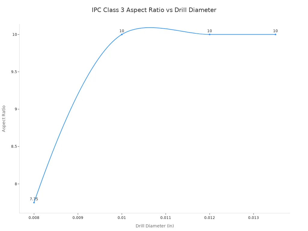
Up to 0.062 in | 0.008 in | 0.023 in | 7.75:1 |
Up to 0.100 in | 0.010 in | 0.025 in | 10:1 |
Up to 0.120 in | 0.012 in | 0.027 in | 10:1 |
Up to 0.135 in | 0.0135 in | 0.028 in | 10:1 |
Aspect ratios also obey the design requirements for Class 3. The chart below shows how the ratio climbs with drill diameter. IPC-6012 prohibits lifted or fractured rings and drill breakouts.
Implementing Via-in-Pad and Blind/Buried Vias
Blind and buried vias improve signal quality. Buried vias connect inner layers without reaching the surface, removing stub effects. Blind vias save space on the opposite outer layer. Back drilling removes unused barrel sections to cut reflections and insertion loss.
These structures carry trade-offs. Buried vias are expensive and hard to inspect. Blind vias need strict registration and plating control. Via-in-pad shortens the signal path, but you must fill it with epoxy to prevent solder flow. Keep digital impedance near 50 ohms. Design validation using test coupons and microsections confirms thermal survival.
Thermal Management Challenges
Heat is the enemy of mission-critical boards. Power components create hot spots that accelerate solder fatigue. Your thermal strategy must spread heat before it damages circuits.
Using Thermal Vias and Metal Core PCBs
Thermal vias move heat away from power components. Too many vias weaken the board. Keep via diameter below 0.3 mm so solder surface tension prevents wicking. Solder mask tenting or plated-over via-in-pad also blocks solder.
Metal core PCBs spread heat differently. The core provides greater structural integrity and thermal conductivity than FR-4. Surface-mount components work best, because they cannot short to the core. In multilayer construction, drill the core and plug it with insulating gel before plating. Anodizing aluminum boosts emissivity and corrosion resistance. You can ground the core to act as a shield.
Integrating Heat Sinks and Thermal Interface Materials
A heat sink is effective only when heat reaches it. Thermal interface materials fill the air gaps between component and sink. Heavy copper traces and ground planes spread heat by conduction. Place thermal pads under hot parts as local spreaders.
Layout also matters. Distribute power components evenly to avoid hotspots. Keep sensitive devices away from heat sources. Put processors near the center so heat scatters in all directions. These actions support long-term reliability while meeting the requirements of the aerospace specification.
Aerospace PCB Assembly Best Practices
Zero-defect aerospace pcb assembly starts with discipline, not inspection. You control process parameters, materials, and environmental conditions at every workstation. All requirements in the quality system exist for one reason: predictable, repeatable output.
Assembly Techniques for Zero-Defect Manufacturing
Cleanliness and Contamination Control
Contamination can bridge fine-pitch conductors and corrupt signals. Flux residue, dust, and ionic debris can short a board silently after years in service. Two standards govern your controls. IPC J-STD-001 defines the manufacturing processes, cleaning requirements, and residue limits. IPC-A-610 defines what the finished assembly must look like.
Standard | Role | Cleanliness Coverage |
|---|---|---|
IPC J-STD-001 | Manufacturing/process standard | Soldering materials, flux-residue limits, cleaning requirements |
IPC-A-610 | Inspection/acceptability standard | Criteria for flux residue, foreign particles, surface debris |
IPC J-STD-001ES | Space addendum | Red plague control plan, flux activity L0–L1, stripper protection |
IPC-A-610 provides criteria for acceptable levels of flux residue, foreign particles, and surface debris. Contamination can create leakage paths and interfere with performance. Class 3 requirements raise the standards for solder joints and component alignment.
These standards frame aerospace pcb assembly. The space addendum J-STD-001ES goes further. You need an approved red plague control plan for silver-coated copper. Flux activity levels must remain within L0–L1. These controls differentiate high-reliability builds from ordinary production.
Advanced Soldering: Selective and Vapor Phase
Selective soldering protects your existing assemblies. A machine-guided nozzle applies solder only to through-hole pins. This approach suits mixed-technology boards with dense component placement. It also limits collateral heat damage.
Vapor phase soldering offers another route to reliability. Condensing vapor transfers heat uniformly across the entire board. The inert atmosphere limits oxidation. A repeatable heating curve minimizes voids and creates consistent joints. Both techniques remove human variability from aerospace pcb assembly.
Communication and Traceability
Rigorous Change Management Process
Process changes carry risk. AS9100 mandates formal configuration management. Engineering change orders control the BOM revision, fabrication drawing revision, and assembly drawing revision. Approved deviations and waivers require documentation before production release.
Configuration baselines protect your program. You prove that each board was manufactured to the approved revision in effect at the time of fabrication. Any design change mid-build triggers a controlled decision. That rigor preserves both reliability and compliance.
Full Material Traceability
AS9100 demands full material traceability. Each batch links to specific laminate lots, solder mask lots, surface finish batches, and solder paste lots. Operator identification, calibration status, and equipment maintenance records complete the picture.
A complete genealogy includes machine programs and process parameters. Each serial number carries AOI, X-ray, and electrical test results. Nonconformance and rework records stay connected to the affected unit. These documentation and traceability systems convert raw material into verified flight hardware. The chain lets you trace root causes quickly after a failure. That speed defines mature aerospace pcb assembly.
Testing and Quality Verification
Electrical Testing and Inspection
Flying Probe and Bed-of-Nails Testing
You verify bare-board integrity before assembly begins. Continuity and isolation tests confirm that your circuit design is intact, with no unexpected connections. Bed-of-nails testing uses a fixture with spring-loaded pins and suits large production runs. Flying probe testing uses moving probes instead of a physical fixture and works best for prototypes and small quantities. As outlined in IPC-9252, continuity must register below 10 ohms for Class 3 boards, providing a standardized benchmark for factory acceptance.
Method | Objective | Relevance to Aerospace PCBs |
|---|---|---|
Bed-of-Nails | In-circuit testing with spring-loaded pins | Verifies connection integrity in high-volume production |
Flying Probe | In-circuit testing without a custom fixture | Ideal for prototypes and small batches |
TDR | Measures trace impedance | Critical for high-speed signal integrity |
Time-Domain Reflectometry (TDR)
TDR injects a fast-rising voltage step onto a conductor and observes the reflections that return. Any abrupt impedance change, such as a connector mismatch or trace-width variation, reflects part of the signal back. The reflection amplitude and polarity reveal the nature of the change, while round-trip travel time gives the distance to the discontinuity. A TDR display plots impedance as a function of electrical distance, giving you a spatially resolved profile of the entire transmission path. This profile verifies that trace impedances meet design targets and screens connectors for solder-void defects.
Advanced Non-Destructive Testing
Automated Optical Inspection (AOI) and X-Ray
AOI handles surface-level defects with visible light and cameras. It catches missing components, solder bridges, and wrong polarity. AOI cannot see under components or within multilayer boards. X-ray inspection fills that gap. 2D X-ray detects BGA voiding and bridging. 3D CT reconstructs layers for void quantification and barrel cracks. AXI measures void percentage against acceptance criteria. A hybrid approach combining both is recommended, with AXI indispensable for aerospace reliability requirements.
Microsectioning and Cross-Sectional Analysis
Microsectioning remains the reference method for plating quality. You mount, grind, and polish a coupon, then examine it under microscopy. This reveals copper thickness, annular ring integrity, and barrel cracks. IPC-6012E qualification for rigid boards demands zero visible defects under microscopy. Microsectioning validates the process, not just the product.
Environmental and Reliability Testing
Thermal Cycling and Thermal Shock
Thermal cycling exposes boards to repeated temperature changes with defined ramp rates and dwell times, often from -40°C to 125°C. High-reliability boards may require hundreds to thousands of cycles. Thermal shock applies rapid transitions to verify resistance to sudden stress. MIL-STD-810 Method 503.7 and DO-160 Section 5 govern these profiles. These tests reveal weak solder joints, laminate delamination, and lifted pads.
Vibration, Mechanical Shock, and Humidity
Vibration profiling reproduces flight mechanical stress and validates solder-joint integrity. Sinusoidal sweeps find resonant frequencies, while random vibration simulates broad-spectrum operational conditions. Mechanical shock testing with high-g launch profiles ensures components and traces remain intact. Humidity testing accelerates corrosion and electrochemical migration. Combined stress testing reveals synergistic failure modes. These protocols form the core of vibration and shock testing for aerospace hardware.
Choosing the Right Manufacturing Partner
Selecting a partner requires more than a certificate. You need a manufacturer who lives by the tough triangle: as9100 quality management, high-reliability fabrication, and environmental survival. The right partner turns stringent requirements into reliable flight hardware.
Beyond the Checklist: What to Look For
Proven Experience with Aerospace Programs
Ask for case studies from your industry. Aerospace and defense projects require PCBs that withstand extreme temperatures, vibration, and radiation while meeting ITAR standards. They often call for ipc class 3 requirements. Case studies prove the manufacturer understands your unique challenges. A partner can show you an HDI control-board for a tightly registered multilayer stack, or an RF module built with low-loss material to a specific impedance requirement. Each project summary should list critical registration controls and released verification results. Each case study should name the program type and the problems solved.
Look past marketing claims. Demand a certificate of conformance, first article inspection reports, and full traceability documentation. Environmental test reports for vibration, thermal cycling, or stress screening matter. Manufacturing travelers and complete audit trails complete the evidence. That documentation set demonstrates aerospace pcb reliability in practice.
In-House Capabilities vs. Outsourcing
Your partner should control its own special processes. Soldering, plating, and coating all affect mission success. Nadcap accreditation validates those processes. In-house capabilities shorten lead times. Outsourcing adds risk and complicates traceability. A manufacturer with internal testing and inspection keeps your data secure under ITAR. Confirm the partner holds ITAR registration and runs a documented compliance program with access controls and annual training.
Evaluating a Partner's Technology Roadmap
Investment in Advanced Equipment
Technology changes quickly in aerospace pcb manufacturing. Evaluate the partner's equipment investments. Look for certification to IPC-1791 and MIL-PRF-31032. These marks signal serious investment. Cybersecurity readiness also matters for defense contracts. Alignment with NIST 800-171 and CMMC requirements protects your technical data. The best partners update equipment to support high-speed materials and fine-pitch assembly.
Commitment to Continuous Improvement
A mature quality system demands continuous improvement. Ask how the manufacturer tracks corrective actions and audit findings. Review operator training records. Look for a quality culture that rejects drift. The partner should invest in new soldering techniques, like selective and vapor phase, to support aerospace pcb assembly. Certification alone cannot guarantee success, but it narrows the field. A roadmap that includes advanced inspection and automation shows long-term dedication. Choose a partner who treats quality as a living system, not a wall plaque. That commitment secures your mission-critical programs.
Aerospace pcb manufacturing in 2026 rests on four pillars. You must meet AS9100D and IPC Class 3 standards. You must select materials that survive -55°C to +125°C and heavy vibration. You must design and assemble boards with zero-defect discipline. You must verify every unit through comprehensive testing.
These requirements are not bureaucratic hurdles. They protect lives and missions. They ensure reliability when failure is not an option.
Success depends on your manufacturing partner. Choose a partner with aerospace pcb assembly experience, proper certification, and a deep commitment to excellence. That partner turns compliance into confidence.
Aerospace technology will keep advancing. PCB manufacturing will evolve with it. Your partner must evolve too.
FAQ
What separates IPC Class 3 from Class 2?
IPC Class 3 demands tighter tolerances for plating thickness, annular rings, and hole quality. These rules apply where failure creates serious safety risks. Class 2 allows looser limits. Aerospace boards must meet Class 3. You cannot field flight hardware with Class 2 workmanship.
Why does AS9100D certification matter for your program?
AS9100D builds on ISO 9001:2015 with aerospace-specific demands. It enforces strict documentation, traceability, and process control. Most aerospace OEMs require this certification from approved vendors. You cannot qualify for government or prime contractor programs without AS9100D.
Which base material handles high temperatures best?
High-Tg FR-4 above 170°C works for many avionics boards. Polyimide offers even greater thermal stability with Tg above 250°C. PTFE suits high-frequency applications but requires specialized lamination. Your material choice must match both thermal and signal requirements.
Should you choose ENIG or ENEPIG?
ENIG provides excellent flatness for fine-pitch parts but carries black pad risk. ENEPIG adds a palladium layer. This layer eliminates black pad and supports universal wire bonding. ENEPIG also withstands more reflow cycles. Choose ENEPIG for mission-critical boards.
How do you prevent solder wicking in via-in-pad?
Fill vias with epoxy before soldering. Keep via diameter below 0.3 mm. Solder surface tension then prevents wicking. Solder mask tenting or plated-over via-in-pad also blocks solder flow. These methods protect joint integrity.
What tests prove aerospace PCB reliability?
Thermal cycling exposes boards to repeated temperature changes, often from -40°C to 125°C. Thermal shock applies rapid transitions per MIL-STD-810 and DO-160. Vibration testing replicates launch and flight conditions. Humidity testing accelerates corrosion and electrochemical migration. Together, these tests reveal weak joints and delamination before deployment.
How does ITAR affect your PCB program?
ITAR registration governs defense-related PCB work. Your manufacturer must hold proper registration before you share controlled information. ITAR compliance requires documented access controls and annual training. Verify registration early to avoid program delays.
