What is Any Layer HDI PCB and What Makes It Unique
You can use any layer hdi pcb for advanced electronics that require tight spacing and superior performance. This technology allows microvias to connect any two layers, setting any layer hdi pcb apart from traditional HDI PCBs.
Feature | Any Layer HDI PCB | Traditional HDI PCB |
|---|---|---|
Layer Connections | Limited via options | |
Trace Spacing | Under 4 mils | 4-8 mils |
LT CIRCUIT is a leader in manufacturing reliable, high-density any layer hdi pcb solutions.
Key Takeaways
Any layer HDI PCBs allow connections between any layers using microvias, offering more design flexibility than traditional boards.
Microvias improve signal quality and reduce noise, making any layer HDI PCBs ideal for high-speed applications.
The compact design of any layer HDI PCBs can reduce board size by 30-50%, fitting more functions into smaller devices.
Any Layer HDI PCB Features
Microvias and Layer Interconnects
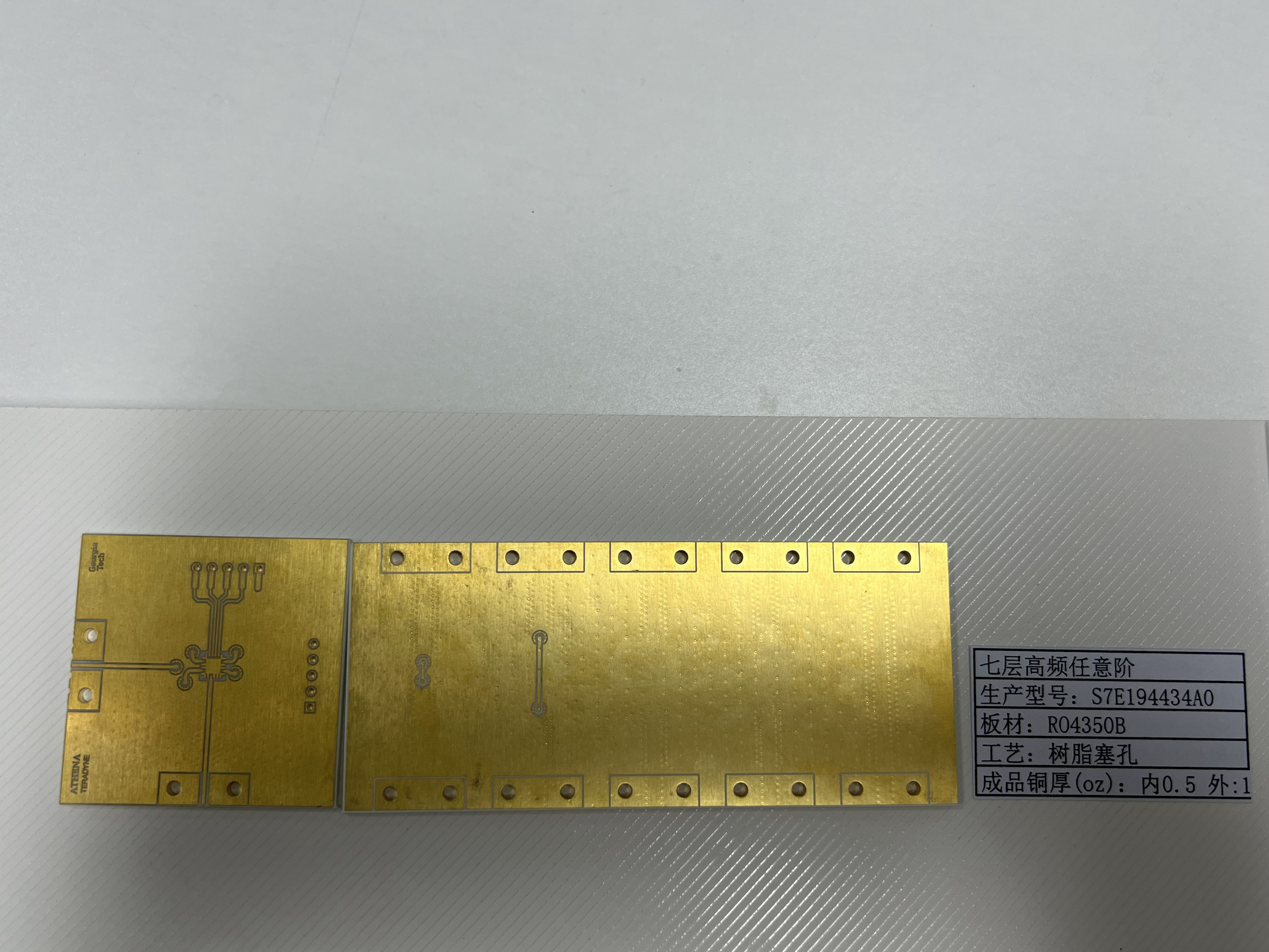
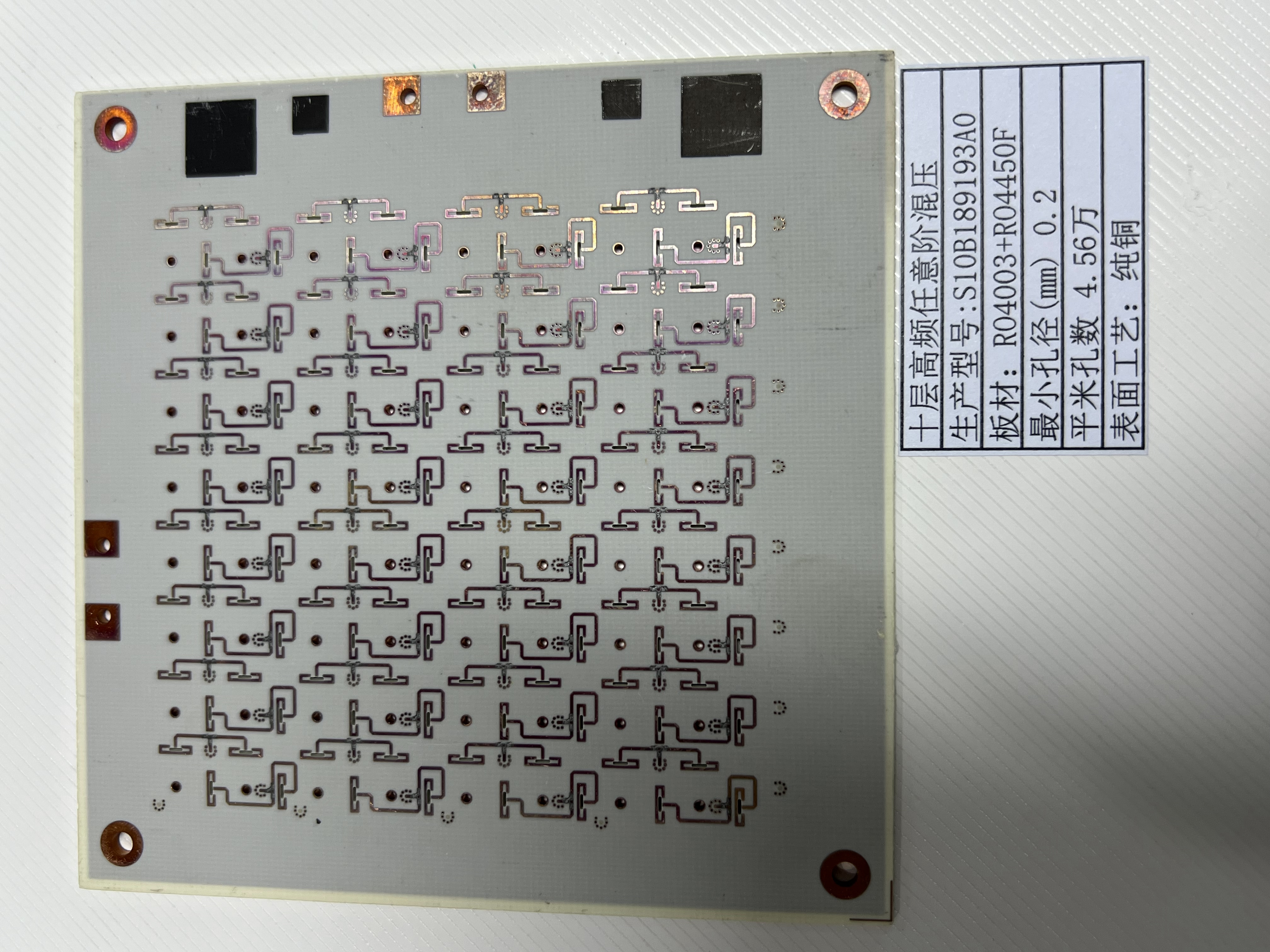
You will notice that any layer hdi pcb stands out because of its advanced use of microvias. These tiny holes, created by laser drilling for vias, connect any two layers in the printed circuit board. This method gives you more design freedom and allows for high-density connections. Microvias are much smaller than traditional through-hole vias, which means you can pack more features into less space. You also get better signal quality because microvias create shorter paths for electrical signals. This reduces signal loss and improves integrity, which is important for high-speed applications.
Microvias also help reduce electrical noise and electromagnetic interference. You get improved performance and reliability in your pcb, especially when you need high-density circuit boards for demanding applications.
Here is a comparison of microvias and traditional through-hole vias:
Aspect | Microvias | Through-Hole Vias |
|---|---|---|
Size | Smaller | Larger |
Aspect Ratio | Up to 20:1 | Lower |
Signal Integrity | Improved | Standard |
Noise Reduction | Enhanced | Limited |
Thermal Management | Better | Standard |
Durability under Stress | Superior | Standard |
LT CIRCUIT uses advanced techniques like UV laser drilling and controlled depth drilling to ensure precise connections between layers. Their expertise in microvia technology means you get a pcb with excellent electrical performance and long-term reliability.
High Density and Compact Design
Any layer hdi pcb technology lets you achieve a much higher density than standard boards. You can use fine-pitch components and stack microvias to connect multiple layers without making the board bigger. This efficient use of space is key for modern devices like smartphones and wearables, where every millimeter counts.
You can reduce pcb size by 30-50% compared to traditional designs.
HDI boards often have 8, 10, or even 20 layers in the same or smaller footprint as a standard 4-6 layer board.
Minimum trace width and spacing can be less than 0.005 inches, and microvias can be as small as 0.008 inches in diameter.
The high density and compact design of any layer hdi pcb allows you to fit more functions into smaller devices, making them ideal for advanced applications in consumer electronics and telecom.
LT CIRCUIT uses advanced materials and manufacturing processes to achieve this level of density. They use sequential lamination, plasma etching, and electroless copper plating to build up layers and ensure strong, reliable connections. Their process supports all available circuit board materials, so you can choose the best option for your application.
Reliability and Performance
You can trust any layer hdi pcb for its outstanding reliability and performance. These boards use low-CTE, high-performance dielectric materials, which handle temperature changes better than standard FR-4 materials. LT CIRCUIT tests every pcb using advanced inspection methods like flying probe testing, AOI, and X-ray analysis. They follow strict industry standards and achieve a 99.8% pass rate, even for complex applications.
Aspect | HDI PCBs | Standard PCBs |
|---|---|---|
Conductor Density | Higher conductor density | Lower conductor density |
Via Density | 5-10 times higher density of vias | Standard via density |
Dielectric Layers | Ultra-thin dielectric layers | Standard thickness dielectric layers |
Thermal Reliability Tests | Temperature cycling tests (-40℃ to +115℃) | Less rigorous thermal testing |
Material Used | Low-CTE high-performance materials | Standard FR-4 materials |
Failure Modes | Microvia connection failures | Through-hole fractures, corrosion |
You will benefit from the doubled lifespan and lower failure rate of HDI boards. LT CIRCUIT’s commitment to quality means your pcb will perform reliably in even the most demanding environments. Their high-density designs and precise layer stacking make them a top choice for applications that require both performance and reliability.
Manufacturing and Advantages with LT CIRCUIT
Any Layer HDI PCB Process
You can see the difference in quality when you look at the manufacturing steps for any layer hdi pcb. LT CIRCUIT uses a precise process to build each printed circuit board. Here is how the process works:
Inner Layer Processing and Imaging: You start with a photoresist layer and use UV light to transfer the circuit pattern.
Sequential Lamination: You build the layers one at a time. This method allows for complex circuits with blind and buried vias.
Microvia Drilling and Formation: LT CIRCUIT uses laser technology to drill microvias. These tiny holes create strong connections between layers.
Copper Plating and Via Filling: You plate the vias with copper to make conductive pathways.
Outer Layer Processing and Solder Mask Application: You process the outer layers and apply a solder mask for protection.
Electrical Testing and Quality Control: LT CIRCUIT tests every pcb to make sure it meets strict standards for electrical performance and reliability.
Final Fabrication and Routing: The panel is routed into individual boards and prepared for shipment.
LT CIRCUIT stands out by using advanced innovations at every step. The company integrates design software that supports any-layer constraints, which helps you reduce design time. In-house R&D teams test new materials and microvia structures, so you get the latest technology in your pcb. Real-time analytics and digital twins monitor the production line, which means you receive consistent quality. LT CIRCUIT also offers embedded component assembly and turnkey testing, giving you a single point of accountability for your high-performance devices.
Description | |
|---|---|
Collaboration with Design Software | Integrates any-layer constraints into PCB layout tools, reducing design iterations and speeding up production. |
In-house R&D Facilities | Prototyping emerging materials and microvia architectures to quickly translate lab breakthroughs into products. |
Advanced Analytics and Digital Twins | Real-time monitoring of production lines to identify yield deviations and optimize processes. |
Value-added Service Diversification | Offers embedded component assembly and turnkey testing solutions for OEMs seeking single-point accountability. |
Advanced Laser Imaging | Upgrades fabrication lines with high-speed laser drills to meet tight tolerances and multilayer requirements. |
Supply Chain Diversification | Collaborates with material developers for optimized substrates and nearshores production to reduce lead times. |
Digital Transformation Initiatives | Implements real-time analytics and predictive maintenance to enhance operational excellence. |
Co-development Agreements | Forges deeper relationships with OEMs to align incentives and unlock new revenue streams. |
You benefit from fast lead times as well. LT CIRCUIT can deliver your HDI pcb in as little as 1–5 days, while traditional boards may take weeks.
Signal Integrity and Space Efficiency
You need strong signal quality and efficient use of space in modern electronics. Any layer hdi pcb technology gives you both. The optimal layer stack-up in these boards improves interference and electromagnetic performance. Controlled impedance routing keeps your signals clear and prevents reflection, which is vital for high-speed data.
Microvias and careful via placement reduce signal disturbance.
Ground planes and spacing between traces lower noise and crosstalk.
A proper power distribution network ensures low noise and stable voltage, which protects signal integrity.
You also get unmatched space efficiency. The compact arrangement of components and interconnections lets you shrink the size of your pcb. Microvias, blind vias, and buried vias allow for higher density connections. You can fit more components into less space, which is perfect for miniaturized design in mobile devices and wearables.
You connect any layer using microvias, blind vias, and buried vias, which increases circuit complexity without making the board larger.
Technologies like microvias and buried vias create intricate signal pathways, keeping the form factor small while maintaining high electrical performance.
Aspect | HDI PCBs | Traditional PCBs |
|---|---|---|
Initial Investment | Higher initial costs | Lower initial costs |
Long-term Reliability | Increased reliability | Standard reliability |
Lifecycle Cost Savings | Significant savings over time | Limited savings |
Performance in Design | Superior performance in tight constraints | Average performance |
Industry Applications
You will find any layer hdi pcb in many advanced applications. The high density and reliable connections make these boards ideal for industries that demand compact size and high performance.
Industry Application | Description |
|---|---|
Consumer Electronics | Dominates the market due to the need for compact, high-density circuit boards in devices like smartphones and tablets. |
Automotive | Rapidly growing sector driven by smart vehicles requiring advanced driver-assistance systems and infotainment. |
Healthcare | Increasing demand for reliable, high-density PCBs in medical devices. |
IT & Telecommunications | Essential for high-speed networking and communication devices. |
Aerospace & Defense | Requires high reliability and performance in critical applications. |
The consumer electronics sector leads the demand for hdi boards, especially in smartphones, tablets, and touch-screen devices.
Automotive applications are growing fast as vehicles become smarter and more connected.
Medical devices, IT, and telecom equipment rely on any layer hdi pcb for their compact size and improved reliability.
HDI technology enables you to design complex circuits for high-performance devices. You can add more features to products like mobile phones, laptops, digital cameras, and 4/5G network equipment. The efficient use of space and high density support the trend toward smaller, more powerful electronics.
You also help the environment by choosing HDI. The compact design reduces material use and makes devices lighter, which can improve battery life and energy efficiency.
With LT CIRCUIT, you get a partner who understands the needs of modern electronics. The company’s expertise in any layer hdi pcb manufacturing ensures you receive boards that meet the highest standards for density, electrical performance, and reliability. You can trust LT CIRCUIT to deliver solutions for your most demanding applications.
You see any layer HDI PCBs driving the future of electronics. Industry experts highlight miniaturization, 5G, and IoT as key trends. The table below shows strong market growth:
Growth Factor | Projected CAGR | Market Size (2032) |
|---|---|---|
~8% | $34.23 Billion |
LT CIRCUIT delivers innovation, advanced manufacturing, and trusted quality for your high-performance needs.
FAQ
What makes any layer hdi pcb different from standard hdi boards?
You can connect all layers using microvias. This gives you more design flexibility. Standard hdi boards only allow limited connections between certain layers.
How do microvias improve hdi pcb performance?
Microvias create short paths between layers. You get better signal quality and less noise. This helps your hdi pcb handle high-speed data and complex layers.
Can you use any layer hdi pcb for devices with many layers?
Yes, you can use any layer hdi pcb for devices with many layers. You can stack up to 20 layers. This supports advanced designs and dense pcb layouts.
See Also
Understanding The Design And Production Of HDI PCBs
Explore Cutting-Edge Techniques For HDI PCB Prototyping
A Look At Common Stack-Up Configurations For HDI PCBs