The Role of Automated Visual Inspection in the Testing Process of PCB Products
Automated visual inspection now transforms pcb inspection in electronics manufacturing. Rising complexity and strict quality demands drive this shift. The AOI market, worth USD 1.16 billion in 2024, is set to reach USD 13.39 billion by 2037.
Statistic Description | Value |
|---|---|
AOI market size (2024) | USD 1.16 billion |
AOI market size (2037) | USD 13.39 billion |
AOI market CAGR (2024-2037) | 20.7% |
LT CIRCUIT leads with advanced automated inspection, moving from manual visual inspection to reliable, efficient pcb testing for printed circuit board quality in electronics.
Key Takeaways
Automated visual inspection uses cameras and software to quickly find tiny defects in PCBs, improving quality and saving money by catching problems early.
This technology works faster and more accurately than manual checks, reducing errors, waste, and production costs while increasing efficiency.
LT CIRCUIT combines advanced inspection tools with strict quality controls to deliver reliable, high-quality PCBs that meet industry standards and customer expectations.
Automated Visual Inspection in PCB Testing
Key Benefits for PCB Inspection
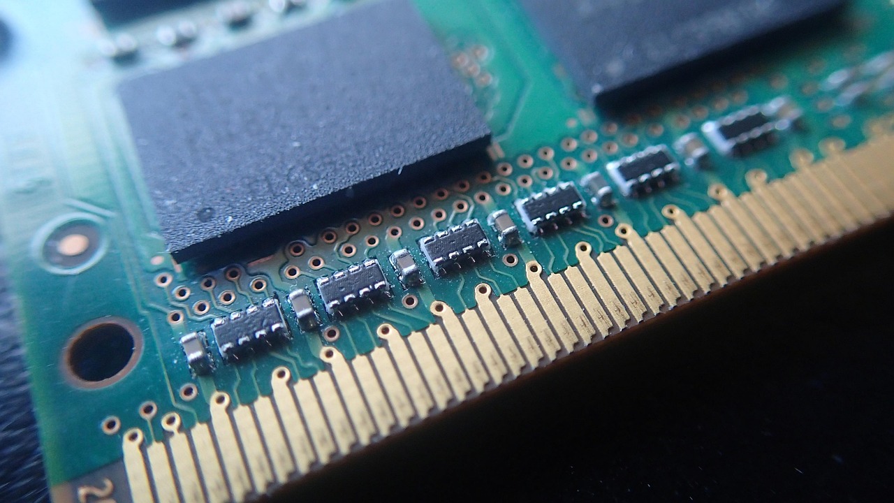
Automated visual inspection has become a key part of modern pcb inspection. This technology uses cameras and software to check printed circuit boards for errors. Automated optical inspection systems can find very small problems, such as stains, missing or misplaced components, soldering flaws, and scratches. These systems work much faster than manual inspection and can check many boards in a short time.
Some main benefits of pcb inspection using automated methods include:
Accurate detection of surface defects and quality-related defects that people might miss.
Real-time error identification, which helps fix problems quickly.
Collection of data for process control and documentation.
Increased production volumes and efficiency by lowering defect rates.
Cost savings compared to other inspection methods, such as X-ray inspection.
Flexible use at different stages of the manufacturing process, including before and after soldering.
Use of advanced imaging and algorithms, like pixel counting and object recognition, to improve defect detection.
Automated visual inspection also improves reliability and accuracy in the inspection process. AOI systems with deep learning can reach accuracy rates above 97%, which means fewer false positives and negatives. This high level of accuracy helps manufacturers deliver high-quality electronics.
Early detection of defects saves money and time. For example, fixing a defect early in the process may cost less than $2, but if the same defect is found after final assembly, the cost can rise to $45. This shows the economic value of early and accurate pcb inspection.
Defects Detected by Automated Systems
Automated inspection systems can find many types of defects during pcb inspection. These include solder shorts, open circuits, missing or misplaced components, and polarity errors. The systems also detect cracks, leakage, and spalling. Advanced AOI can measure the height and shape of components, which helps find problems that affect the reliability of the printed circuit board.
Aspect | Details |
|---|---|
Crack, Leakage, Spalling | |
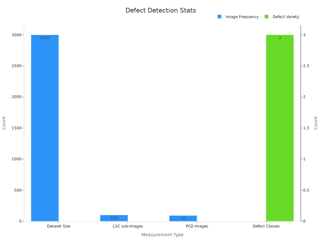
Dataset Size | 3,000 annotated images (training, validation, test split 7:2:1) |
Sub-Images Created | 100 sub-LSC images (800×800 pixels), 92 PCD images (5,000×5,000 pixels) |
Data Augmentation | Rotation, scaling, flipping, brightness adjustment (50% probability) |
Annotation Details | Bounding boxes, segmentation points, defect category (crack, leakage, spalling) |
Detection Performance | Crack detection better on LSC images; leakage and spalling slightly better on PCD images |
Automated optical inspection systems use methods such as template matching and vectoral imaging to improve the detection of defects. These methods of automated optical inspection help catch both common and rare problems. By finding defects early, manufacturers can reduce rework, lower waste, and prevent defective pcbs from reaching customers. This leads to better quality and fewer returns.
LT CIRCUIT’s Approach to Quality
LT CIRCUIT stands out in electronics manufacturing by using advanced automated visual inspection and strict quality control. The company uses statistical process control and Pareto analysis to find and reduce defects early in the pcb inspection process. LT CIRCUIT sets design rules for test points and reviews design files before manufacturing. This helps prevent costly errors and ensures the quality of every printed circuit board.
The company tracks defect reduction, yield rates, and quality control efficiency. Automated and manual inspection methods, including AOI and X-ray inspection, help find both surface defects and hidden problems. LT CIRCUIT holds important certifications, such as RoHS, UL, and ISO 9001, which show its commitment to quality.
Precision drilling accuracy rates exceed 95%, meeting high standards for mechanical reliability.
Plating quality is checked with control charts to keep the process stable.
Soldering uses temperature-controlled irons and lead-free solder for strong joints.
Electrical testing checks all connections to make sure the pcb works as designed.
Thermal management testing ensures the board can handle heat and high current.
By combining automated visual inspection with strong process controls, LT CIRCUIT delivers reliable, high-quality electronics. The company’s approach reduces the risk of quality-related defects and supports customer satisfaction in every project.
Challenges in PCB Inspection and Solutions
Common Testing Challenges
PCB inspection faces many challenges as electronics become more complex. Manufacturers must check for tiny defects in high-density boards. These boards often have many layers and small parts. Some common challenges in pcb inspection include:
False positives, where the system marks a defect that does not exist. This causes extra work and higher costs.
False negatives, where real defects go unnoticed. These can lead to faulty products reaching customers.
Fast inspection speed is needed in high-volume production. Rushing can lower accuracy and create bottlenecks.
Imaging resolution may not catch small or subtle defects, which is important for industries like semiconductors.
Detection algorithms sometimes miss defects or need more training to work well.
PCB complexity increases with more components and layers, making inspection harder.
These challenges can raise error rates and make the inspection process more difficult. They affect quality and efficiency in electronics, automotive, and medical device manufacturing.
Automated vs. Manual Inspection
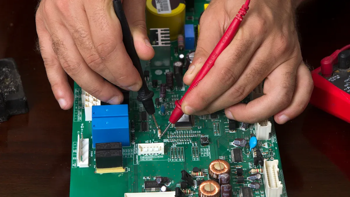
Manual inspection relies on people to find defects. This method is slow and can miss problems because of fatigue or human error. Automated optical inspection uses cameras and software to check each pcb quickly and accurately. Automated systems find small defects that people might miss. They also work faster and do not get tired.
Automated inspection reduces waste and rework costs by catching issues early.
It provides detailed records, helping teams improve the process.
Faster inspection means more pcbs can be tested in less time, lowering labor costs.
Manual inspection often leads to higher costs and more missed defects.
Automated inspection gives a clear advantage in speed, accuracy, and cost savings.
LT CIRCUIT’s Solutions for Reliable PCB Testing
LT CIRCUIT uses advanced technologies to solve challenges in pcb inspection. The company combines automated optical inspection with strict process controls. This approach helps detect defects early and ensures high quality. LT CIRCUIT invests in high-resolution imaging and smart algorithms to improve detection rates. The team reviews design files before production to prevent errors. They also track inspection data to find and fix problems quickly.
By focusing on quality and customer satisfaction, LT CIRCUIT delivers reliable pcb testing for many electronics industries. Their solutions help reduce errors, improve efficiency, and support strong product performance.
Automated visual inspection brings many benefits to pcb manufacturing.
High-speed cameras and software find defects early, saving costs and improving quality.
Consistent inspection increases customer trust and satisfaction.
The market for these systems keeps growing as technology advances.
FAQ
What is automated visual inspection in PCB testing?
Automated visual inspection uses cameras and software to check PCBs for defects. The system finds errors quickly and helps improve product quality.
How does automated inspection improve PCB quality?
Automated inspection finds small defects early. This process reduces waste and prevents faulty boards from reaching customers. Manufacturers see better product reliability.
Why do manufacturers choose LT CIRCUIT for PCB testing?
LT CIRCUIT uses advanced inspection tools and strict quality checks. Customers trust the brand for reliable, high-quality PCB products.
See Also
Essential Techniques For Achieving Quality Control In PCB Production
Vacuum Two-Fluid Etching Machines Driving Precision In PCB Fabrication
Step-By-Step Guide To The PCB Manufacturing Workflow
How LDI Technology Enhances The Quality Of PCB Products
Key Quality Control Measures For Heavy Copper PCBs In Automotive Electronics