What Is the Difference Between Base and Finished Copper on PCBs
The main distinction in base vs finished copper on PCB becomes clear when you compare the original copper layer to the final thickness after all manufacturing processes. This difference is important because the copper thickness directly impacts both performance and reliability.
PCBs with substantial copper layers manage heat efficiently and enhance electrical performance.
High thermal conductivity is essential for supporting high-frequency and high-heat components.
Understanding base vs finished copper on PCB helps you select the right board for your power, signal, and mechanical requirements. LT CIRCUIT ensures precise control over both base and finished copper thickness, providing you with the optimal PCB solution for your needs.
Key Takeaways
Base copper is the original layer received from suppliers, while finished copper is the final thickness after manufacturing. Understanding this difference is crucial for selecting the right PCB.
Thicker copper layers improve performance by reducing resistance and managing heat better. Always match copper thickness to your application’s power and thermal needs for optimal results.
LT CIRCUIT uses advanced technology to ensure precise control over copper thickness, enhancing the reliability and performance of your PCBs.
Base vs Finished Copper on PCB
Definitions
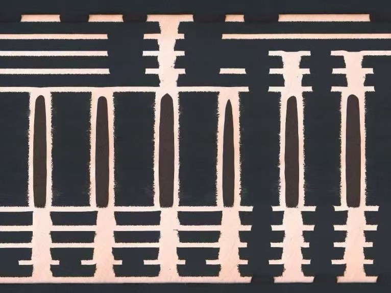
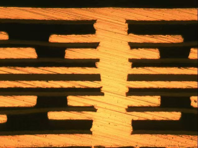
When you compare base vs finished copper on pcb, you need to understand what each term means. Industry standards like IPC-4562 and IPC-A-600 help you define these terms clearly. Base copper refers to the original copper layer that you receive from suppliers. Finished copper describes the final thickness of copper after all manufacturing steps, including plating and etching, are complete. The difference between base vs finished copper on pcb comes from the extra copper added or removed during production.
Here is a table that shows the official definitions:
Type of Copper | Definition |
|---|---|
Base Copper | The copper thickness as received from suppliers, originally defined by weight (oz/ft²) but now commonly measured in micrometers (µm). |
Finished Copper | The final thickness of copper on the completed PCB, which may vary based on manufacturing processes. |
You need to pay attention to base vs finished copper on pcb because the final copper thickness affects how your circuit board performs. The finished copper layer determines how much current your pcb can carry and how well it manages heat.
Measurement Standards
You measure copper thickness in several ways. Most pcb manufacturers use ounces per square foot (oz/ft²), micrometers (µm), millimeters (mm), or inches. You often see copper thickness listed in the stack-up files for each pcb layer. You can check copper thickness by asking your supplier, looking at the fab drawing, or using physical testing methods.
Here is a table that shows common copper thickness measurements:
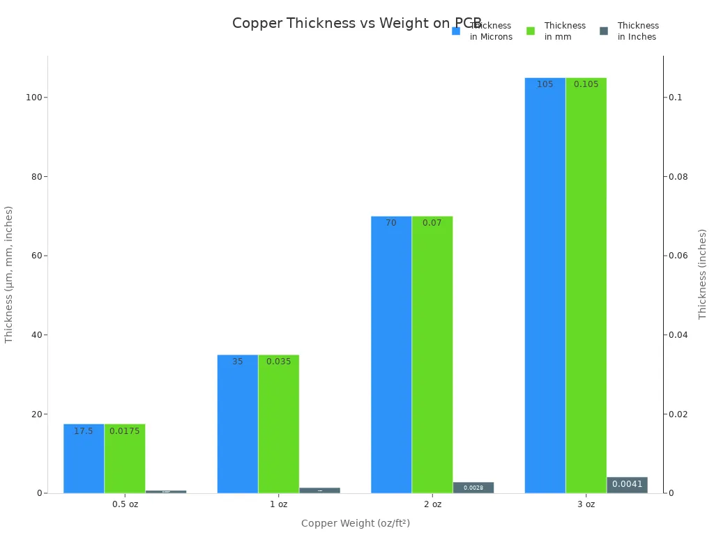
Oz (ounce/ft²) | Microns (µm) | Millimeters (mm) | Inches |
|---|---|---|---|
17.5 µm | 0.0175 mm | 0.0007” | |
1 oz | 35 µm | 0.035 mm | 0.0014” |
2 oz | 70 µm | 0.070 mm | 0.0028” |
3 oz | 105 µm | 0.105 mm | 0.0041” |
You can also use other units. For example, 1 mil equals 25.4 µm. Many pcb designs use 18 µm as a common copper thickness.
Measurement Unit | Conversion to Micrometers (µm) | Notes |
|---|---|---|
1 mil | 25.4 µm | Commonly used for thickness and spacing. |
1 oz/sq ft | 35 µm | Used to measure copper layer thickness. |
Common thickness (H) | 18 µm | Represents a typical copper thickness. |
You should know that copper thickness can vary. For 0.5 oz and 1 oz copper, the tolerance is usually ±10%. For 2 oz or higher, the tolerance is ±15%.
±10% for 0.5 oz and 1 oz
±15% for 2 oz or higher
LT CIRCUIT’s Approach
You want your pcb to have reliable copper thickness and high quality. LT CIRCUIT uses advanced technology to control copper thickness during production. The brand applies vertical continuous plating to keep copper layers consistent across every pcb. LT CIRCUIT adjusts bath temperature and controls copper ion diffusion to form uniform layers. Real-time monitoring and cyclic voltammetric stripping help maintain the right copper thickness and quality.
LT CIRCUIT also follows strict quality assurance steps. The company prepares surfaces carefully before adding copper. It monitors metal ion concentrations and bath temperatures during ENIG manufacturing. LT CIRCUIT uses X-ray fluorescence spectroscopy (XRF) to check coating thickness. The team receives regular training to keep standards high.
You can choose from LT CIRCUIT’s wide range of products, including HDI PCB boards, multilayer PCB boards, and advanced HDI any layer PCBs. Each product offers options for copper thickness, surface finishes, and solder mask colors. LT CIRCUIT’s expertise in base vs finished copper on pcb ensures that you get a circuit board that meets your needs for performance and reliability.
Practical Impact
Performance
Copper thickness plays a major role in how your pcb performs. When you choose thicker copper, you lower DC resistance, which helps your circuit board distribute power efficiently and reduces voltage drop. You also increase the current carrying capacity, so your pcb can handle higher loads without overheating. Thicker copper spreads heat more evenly, preventing hotspots and keeping components safe. For example, a 2 oz copper layer can lower temperature rise compared to a 1 oz layer, which is important for power ICs and high-frequency designs. Stronger via holes from thicker copper also improve reliability, making your pcb less likely to crack or fail under stress.
Tip: Always match copper thickness to your application’s power and thermal needs for best results.
Manufacturing
You face several challenges when manufacturing pcbs with precise copper thickness. Uniform plating is difficult, especially in multilayer boards with high aspect ratio holes. Non-uniform plating, voids, and excessive copper can affect quality. LT CIRCUIT uses pulse plating and direct metallization to keep copper thickness accurate within tight tolerances. Enhanced etching techniques help maintain trace width, while controlled pressure lamination reduces delamination. These advanced processes ensure your pcb meets strict standards for reliability and performance.
LT CIRCUIT offers copper weights from 1 to 6 ounces, giving you flexibility for different current capacities and thermal requirements.
Specialized manufacturing supports high-power and high-frequency applications, such as EV inverters and aerospace systems.
Application Choices
Selecting the right copper thickness depends on your application. For general-purpose pcbs, 1 oz copper provides a good balance of cost and performance. Power electronics often need 2 oz or more for better thermal management and lower resistance. Specialized boards, like HDI and multilayer pcbs, require careful control of copper thickness for mechanical stability and heat dissipation.
Copper Thickness | Common Applications | Key Considerations |
|---|---|---|
1 oz | General-purpose pcb | Cost-effective, reliable |
2 oz | Power electronics | Improved heat dissipation, lower resistance |
3 oz+ | Specialized applications | Needs advanced manufacturing |
LT CIRCUIT’s product range includes HDI, multilayer, and any layer pcbs. For example, a 6-layer automotive ECU pcb uses copper balancing to prevent warping from engine heat, while an 8-layer HDI pcb for smartphones relies on precise copper thickness to avoid twisting during soldering. By choosing the right copper thickness, you ensure your circuit board meets the demands of your industry.
You need to know the main differences between base and finished copper on a pcb. The table below shows how exposed copper and bare copper compare in design and cost.
Feature | Exposed Copper on PCB | Bare Copper PCB |
|---|---|---|
Definition | Parts of the board are uncovered for specific use | Entire copper area is exposed without protection |
Surface Finish | May have protective finishes like ENIG, HASL | No surface finish, prone to oxidation |
Cost | Generally more expensive due to finishes | Cheaper but requires careful handling |
Usage | Part of a planned design | Used in specific applications requiring bare copper |
Accurate copper thickness helps you control impedance, improve reliability, and avoid costly failures. You should specify copper thickness in mils or micrometers for best results. If you want a pcb that matches your needs, LT CIRCUIT can help you choose the right solution.
FAQ
What is the main difference between base copper and finished copper on a PCB?
You see base copper as the original layer. Finished copper includes all plating and etching steps. Finished copper determines your board’s final electrical and thermal properties.
How do you choose the right copper thickness for your PCB application?
You match copper thickness to your current, heat, and reliability needs.
LT CIRCUIT offers options from 1 oz to 6 oz for different applications.
Does LT CIRCUIT provide custom copper thickness for specialized projects?
Option | Availability | Benefit |
|---|---|---|
Custom Thickness | Yes | You get tailored PCBs for your unique requirements. |
See Also
Understanding OSP Finishes: Advantages and Challenges for PCB Makers
Expert Techniques for Effective Immersion Tin Finishing in PCBs
Comprehensive Guide to Production Technologies for Heavy Copper PCBs
Key Design Strategies for High Current Heavy Copper PCBs
Utilizing Panasonic Copper-Clad Laminates in PCB Production Processes