The benefits of using LDI exposure machines to produce circuits for HDI PCB products
Laser Direct Imaging (LDI) has transformed the way circuits are manufactured, showcasing the benefits of using LDI by eliminating the need for photomasks, which reduces costs and minimizes errors. This enhanced accuracy facilitates the creation of intricate circuits for modern devices. Additionally, LDI consumes less energy, leading to cost savings while maintaining high quality. It enables faster prototypes and rapid design updates, significantly improving production speed. These benefits of using LDI underscore its importance in the production of high-quality HDI PCBs.
Key Takeaways
LDI technology improves accuracy in making PCBs, allowing detailed designs with fewer mistakes.
Using LDI lowers costs by removing the need for photomasks. This creates less waste and is better for the environment.
LDI makes prototyping and production faster, helping meet market needs quickly.
LDI can handle large-scale production while keeping quality the same for big orders.
LT CIRCUIT uses LDI to make strong, high-quality HDI PCBs for many industries.
Understanding LDI Technology and Its Role in HDI PCB Manufacturing
What is Laser Direct Imaging (LDI)?
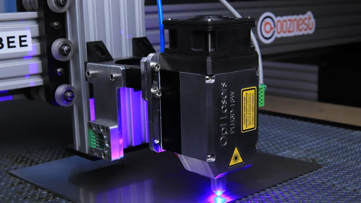
Laser Direct Imaging (LDI) is a modern way to make circuit patterns on printed circuit boards (PCBs) using lasers. Unlike older methods that need photomasks, LDI uses focused lasers to directly expose the photoresist layer on the PCB. This method is very accurate and helps create detailed designs needed for high-density interconnect (HDI) PCBs.
Here’s how LDI works:
Lasers shine light at specific wavelengths, like UV or blue, to match the photoresist.
Special optics adjust the laser’s size and focus for clean exposure.
A scanning system moves the laser across the PCB for even exposure and fewer mistakes.
High-precision stages hold the PCB steady, helping create complex designs.
The process starts with cleaning the surface, adding a photosensitive layer, and exposing it to the laser to form the circuit.
This advanced method avoids many problems of older photolithography techniques, making it perfect for today’s electronics.
Why HDI PCBs Need Better Imaging Methods
HDI PCBs are important for small, powerful devices we use today. These boards have tiny lines, microvias, and many layers, needing very precise imaging. Older methods often can’t handle these needs.
The demand for smaller, energy-saving devices, like those in medical tech, has increased the need for HDI PCBs. These boards allow fast connections and dense layouts, making them key for advanced uses. The HDI PCB market offers many options with different layers, materials, and finishes. New imaging and manufacturing methods are needed to meet these demands.
How LT CIRCUIT Improves HDI PCB Production
LT CIRCUIT is helping change how HDI PCBs are made. By using LDI technology, they create high-quality PCBs with great accuracy. LT CIRCUIT focuses on new ideas to meet the needs of industries like electronics, telecom, and aerospace.
The company uses advanced materials and processes to make reliable PCBs. With a focus on happy customers, LT CIRCUIT leads in offering top solutions for HDI PCB production.
Key Benefits of Using LDI for HDI PCB Production
Better accuracy for detailed designs
Making HDI PCBs needs great accuracy. These boards have tiny lines and spaces for modern devices. Laser Direct Imaging (LDI) is very precise. It uses lasers to directly expose the photoresist layer. This makes sure circuits are aligned and sharp.
Here’s how LDI compares to older methods:
Feature | LDI Technology | Older Methods |
|---|---|---|
Line Width | Can do 50/50 µm and 25/25 µm | Handles only wider lines |
Speed | Makes 1,400 panels daily | Slower production |
Complexity | Handles dense patterns well | Struggles with complex designs |
LDI works well for HDI PCBs. For instance, with 9 W laser power and five heads, it can process 1,400 panels daily. This ensures even tough designs are made quickly and accurately.
Saves money by reducing waste
LDI helps save money by cutting waste. Old methods use photomasks, which are expensive and thrown away after use. LDI skips photomasks, lowering costs and helping the environment.
Here’s how LDI saves resources:
Uses 30–40% less solvent for 1,000 boards.
Avoids 15–20 kg of mask waste per batch.
Using LDI means less waste and a greener process. It’s a smart and cost-saving choice for making HDI PCBs.
Fewer mistakes and better results
Mistakes in PCB making can be costly. LDI reduces errors and improves results. Its precision ensures circuit patterns are made correctly, cutting down on defects.
Here are some quality stats with LDI:
Metric | Value Range |
|---|---|
First Pass Yield (FPY) | |
Defects Per Million Opportunities (DPMO) | 500 to 1000 |
Customer Return Rate | Less than 1% |
These numbers show how LDI improves quality. More good boards are made on the first try. Fewer defects mean happier customers. LDI keeps production smooth and reliable for HDI PCBs.
Faster prototyping and production cycles
Speed matters when making HDI PCBs. A quick process is needed to go from design to production. Laser Direct Imaging (LDI) machines help by cutting down prototyping and production times. Unlike older methods that use photomasks, LDI uses lasers to expose the photoresist layer directly. This skips steps, saving time and speeding up the process.
LDI works well for detailed designs. For example, it handles line and space designs smaller than 75µm. These machines can expose up to 90–120 panels per hour. Even for tricky designs needing tight alignment, LDI stays efficient. Older imaging methods may only manage 60 panels per hour. Advanced LDI machines keep speed high without losing quality. This makes LDI great for industries needing fast prototyping and production.
Using LDI lets you meet market needs faster. Whether creating a new device or improving an old one, quick prototyping and production give you an advantage. LDI is not just fast; it also ensures accuracy and dependability during production.
Scalability for high-volume manufacturing
As production grows, scaling up becomes important. LDI technology helps with large-scale manufacturing by boosting efficiency and handling complex designs. This is key for HDI PCBs, which need detailed patterns and precise imaging.
Modern LDI systems use advanced tools like multi-wavelength lasers and better optics. These upgrades make it easier to produce high-density PCBs with steady quality. Faster imaging speeds and sharper resolution improve scalability, helping meet tight deadlines for big orders.
Here’s how LDI supports scaling:
It speeds up production cycles, saving time.
It handles detailed designs well, keeping results consistent in big batches.
It makes high-density PCBs, meeting needs in industries like telecom and aerospace.
LDI lets manufacturers grow without losing quality. It’s a smart choice for meeting the rising demand for HDI PCBs. With LDI, you get more output, lower costs, and better reliability for large-scale production.
Comparing LDI Technology with Traditional Photolithography
Challenges of Traditional Photolithography for HDI PCBs
Traditional photolithography has been used for years to make PCB circuits. But it struggles to meet the needs of modern HDI PCBs. This method uses photomasks, which are templates for transferring patterns onto PCBs. These masks come with several problems:
Accuracy Issues: Photomasks can’t handle very small designs, like lines under 50 µm.
High Costs: Making and maintaining photomasks is expensive for manufacturers.
Time-Consuming: Creating and aligning photomasks takes a lot of time.
Limited Flexibility: Photomasks can’t easily adapt to design changes.
Environmental Sensitivity: Photolithography needs controlled conditions to avoid defects from heat or humidity.
These problems make photolithography less useful for the precise and flexible needs of HDI PCBs.
How LDI Overcomes These Challenges
Laser Direct Imaging (LDI) solves these issues by using lasers to directly create PCB patterns. This method doesn’t need photomasks, offering many benefits:
Enhanced Precision: LDI creates very detailed designs with sub-micron accuracy.
Cost Efficiency: Without photomasks, LDI lowers costs and reduces waste.
Faster Production: LDI speeds up prototyping and shortens production times.
Flexibility in Design: LDI allows quick design changes, perfect for small production runs.
Improved Quality: Direct imaging reduces errors, making better-quality PCBs.
Here’s a comparison of LDI and traditional photolithography:
Feature | LDI Technology | Traditional Photolithography |
|---|---|---|
Accuracy | Struggles with complex designs | |
Flexibility | Easy to adjust designs | Hard to change due to masks |
Cost | Lower costs without masks | Higher costs with mask usage |
Implementation Time | Faster production cycles | Slower due to mask setup |
Complexity Handling | Handles intricate designs well | Struggles with detailed patterns |
LDI has become a key tool for making HDI PCBs by solving these challenges.
Why LT CIRCUIT Relies on LDI for Superior Results
LT CIRCUIT uses LDI technology to make top-quality HDI PCBs. This choice is based on the many advantages of LDI:
Advantage | Description |
|---|---|
Precision and Accuracy | Creates detailed designs with perfect alignment and control. |
Flexibility and Design Agility | Speeds up prototyping and lowers costs by skipping photomasks. |
Quality and Yield Improvement | Reduces defects and improves the number of good boards made. |
Environmental and Cost Efficiency | Uses fewer chemicals and saves energy, supporting eco-friendly practices. |
Support for Advanced PCB Technologies | Makes complex designs needed for smaller, high-performance devices. |
Scalability and Future-Proofing | Works with new materials and adapts to future manufacturing needs. |
By using LDI, LT CIRCUIT ensures its HDI PCBs are precise, reliable, and high-quality. This makes them a trusted choice for industries like telecom, aerospace, and electronics.
LDI offers more than just cost savings and precision. It also supports green practices and helps LT CIRCUIT lead in innovative PCB production.
Real-World Uses of LDI in Making HDI PCBs
Uses in gadgets and mobile devices
Laser Direct Imaging (LDI) is key for making HDI PCBs in gadgets and phones. These products need small, powerful circuit boards with detailed designs. LDI helps meet these needs with great accuracy and speed. It directly creates PCB patterns without needing photomasks. This allows for smaller, more complex designs with tightly packed parts.
Evidence Description | Key Insights |
|---|---|
Growth in the DMD 405nm segment | Expected to lead due to its flexibility in HDI PCB uses. |
LDI market value by 2025 | Predicted to reach $708.2 million, driven by precise PCB needs. |
HDI PCB use in gadgets and cars | Growing need for accurate imaging for complex designs. |
The demand for advanced phones, smartwatches, and IoT devices shows why LDI is important. Its ability to make detailed circuits ensures these devices work well while staying small.
Uses in cars and airplanes
The car and airplane industries depend on LDI for HDI PCBs. These fields need very precise parts for safety and performance. LDI provides accurate and dependable imaging for these needs.
Cars benefit from LDI as electric vehicles (EVs) and driver-assist systems grow. These systems need exact electronic parts to work properly.
In airplanes, LDI is crucial for making avionics parts where accuracy is vital. High-precision imaging ensures these parts meet strict rules.
By solving these industries' challenges, LDI has become essential for new ideas in cars and airplanes.
How LT CIRCUIT leads in HDI PCB trends
LT CIRCUIT stays ahead by using LDI with new HDI PCB trends. The company works on innovations like Metal Core PCBs (MCPCBs), which improve heat control and electrical performance. These are especially useful in high-power uses like electric cars.
With LDI, LT CIRCUIT ensures its products meet the changing needs of gadgets, cars, and airplanes. This focus on new ideas makes LT CIRCUIT a leader in HDI PCB production, offering solutions that are precise, reliable, and efficient.
Using LDI machines for HDI PCB production has many advantages. They offer great precision, faster production, and less material waste. This ensures high-quality PCBs every time. LT CIRCUIT leads the way by using LDI to make advanced and reliable PCBs that fit your needs.
The future of LDI technology is bright, with big growth expected:
The LDI market could grow from $800 million in 2023 to $1.45 billion by 2032, with a yearly growth rate of 6.7%.
The global LDI market may expand at a yearly growth rate of 10% by 2030, thanks to more automation in factories.
The LDI equipment market might reach $2.5 billion by 2033, growing at a yearly rate of 9.0% from 2026 to 2033.
These improvements will keep changing the electronics world. They will help you meet future technology needs with ease and confidence.
FAQ
1. Why is LDI technology better for making HDI PCBs?
LDI is very accurate and doesn’t need photomasks. This lowers mistakes and waste. It helps create detailed designs faster, perfect for HDI PCBs.
2. How does LDI help save money during production?
LDI skips using photomasks, cutting material costs. It also uses fewer chemicals, reducing waste. This saves money while keeping quality high.
3. Can LDI make complicated PCB designs?
Yes, LDI is great for tricky patterns. Its lasers are very precise, making it perfect for microvias and tiny line spaces in HDI PCBs.
4. Is LDI good for making lots of PCBs?
Yes! LDI works well for big orders. It keeps quality steady, even for large batches, making it ideal for industries like telecom and aerospace.
5. Why does LT CIRCUIT choose LDI for HDI PCBs?
LT CIRCUIT uses LDI to make accurate and eco-friendly PCBs. It saves money, supports new ideas, and ensures top quality for their customers.
See Also
How LDI Applications Enhance PCB Product Quality Significantly
Explore Cutting-Edge HDI PCB Prototyping Methods Right Now
Quick Turn HDI PCBs: A Cost-Saving Solution for 2025 Projects
Utilizing Horizontal Copper Sinking Technology for PCB Manufacturing