Key Differences Between Blind Vias Buried Vias and Through-Hole Vias
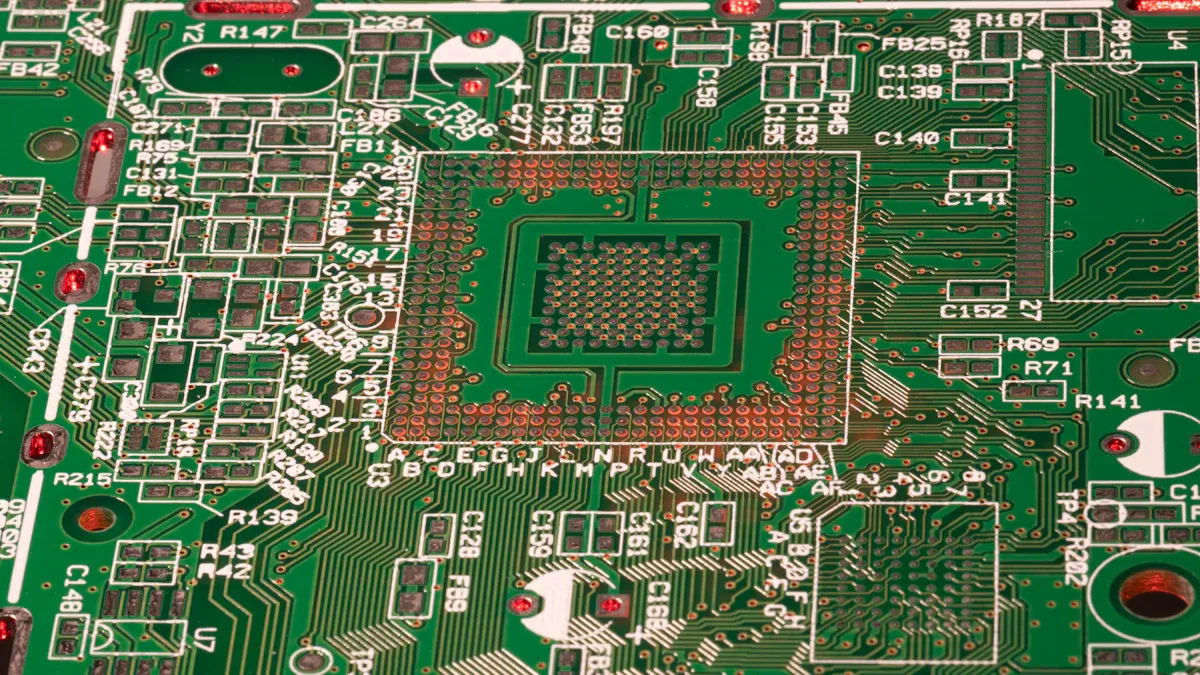
Vias are small holes in a circuit board that connect different layers of the board. Blind buried hole circuit boards utilize blind vias, which join an outer layer to an inner one without going through the entire board. Buried vias, on the other hand, are hidden between the inside layers of the board. Through-hole vias pass completely through the board. Each type has special features and purposes, and choosing the right via affects how well the board works and its cost. For blind buried hole circuit boards, selecting the appropriate via helps save space and ensure good connections.
Key Takeaways
Learn about three types of vias: blind vias join outer layers to inner ones, buried vias connect only inner layers, and through-hole vias go through the whole board.
Use blind or buried vias in tight designs to save space and make signals better, like in phones and tablets.
Think about how they are made; blind and buried vias need special methods, so check if your PCB maker has the right tools and knows how to do it.
Compare cost and benefits; through-hole vias cost less, but blind and buried vias work better in small designs.
Test samples first to find problems with vias before making many, so your final product works well and lasts long.
Blind Vias in PCB Design
What Are Blind Vias?
Blind vias are small holes in a PCB that link the outer layer to one or more inner layers. They do not go through the whole board. These vias are very useful in multi-layer PCB designs, especially when space is tight. Unlike through-hole vias, blind vias stop inside the board. This makes them great for high-density connections.
Blind vias are made using methods like laser or mechanical drilling. They are important in high-density interconnect (HDI) PCBs, where small designs need smart use of space. For example, smartphone motherboards often use blind vias to fit many connections in a small area.
Description | |
|---|---|
Photo Defined Blind Via | Made by adding a photosensitive resin to a core. Paths are created after etching and plating. Common in multilayer organic BGA packages and cell phone PCBs. |
Sequential Lamination Blind Via | Built by processing a thin laminate through two-sided PCB steps. This method costs more due to extra steps and lower yield. Used in older cell phone PCBs. |
Controlled Depth Drilled Blind Via | Made like through-hole vias but drilled partway into the PCB. This allows controlled connections without touching deeper layers. |
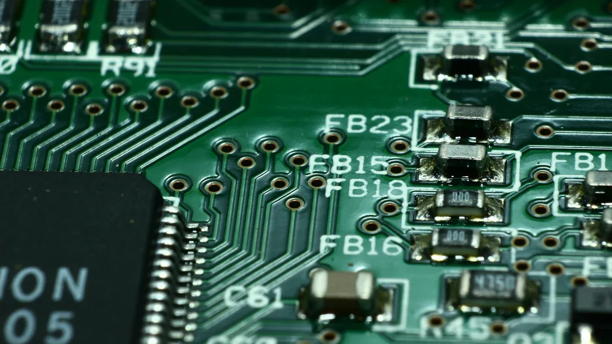
Characteristics of Blind Vias
Blind vias have special features that make them great for advanced PCB designs. They connect specific layers without affecting others. This helps make the board layout better. They also lower parasitic capacitance, which improves signal quality and performance.
Blind Vias | Through Hole Vias | |
|---|---|---|
Insertion Loss | Lower | Higher |
Impedance Discontinuity | Improved | Standard |
Signal Strength | High | Moderate |
Attenuation | Minimal | Higher |
Change in Impedance | 46-52 | 42-53 |
Return Loss | 4 dB - 8 dB | 40 GHz - 80 GHz |
Operational Bandwidth | Wider | Narrower |
Efficiency in Heat Dissipation | Improved | Standard |
Blind vias also help with heat dissipation better than through-hole vias. This is useful for high-speed signal applications, like graphics card PCBs. By lowering the number of layers, blind vias make designs cheaper and more efficient.
Advantages of Blind Vias
Blind vias have many benefits that make them important in modern PCB designs:
Space Optimization: Blind vias save space on the top layer. This allows better placement of parts and routing on lower layers.
Improved Signal Integrity: Blind vias reduce parasitic capacitance. This boosts signal strength and lowers signal loss.
High-Density Routing: They allow compact designs, making them perfect for devices like smartphones and tablets.
Enhanced Performance: Blind vias work well for high-frequency uses by creating short, direct paths between layers.
Application | Advantages |
|---|---|
Smartphone Motherboards | High-density routing with laser-drilled vias of 0.15-0.2mm in diameter. |
Graphics Card PCBs | Ensures high-speed signal transmission by linking GPU chips with inner layers. |
Blind vias also reduce the number of layers in HDI PCBs, making manufacturing easier and cheaper. For example, in one case study, blind vias solved routing problems for power management ICs and processors. This led to better designs.
Tip: When designing a PCB, think about using blind vias. They save space and improve performance, especially in high-density or high-frequency designs.
Disadvantages of Blind Vias
Blind vias have many benefits, but they also have downsides. These issues can affect the cost, difficulty, and reliability of your PCB.
Higher Manufacturing Costs
Making blind vias needs advanced methods like laser drilling. These methods cost more than making through-hole vias. If your design uses many blind vias, the total cost can go up a lot.Complex Fabrication Process
Blind vias need careful drilling and plating. This makes the process harder and takes more time. It can also lower the number of good boards made. You must work closely with your PCB maker to match their skills.Limited Depth
Blind vias cannot go too deep into the board. The depth and width must stay balanced to keep the board strong. This limit can make them less useful for designs needing deep connections.Potential Reliability Issues
Poorly made blind vias can have problems like gaps or bad plating. These problems can hurt how well your PCB works and how long it lasts. To avoid this, make sure your PCB maker has strict quality checks.
Note: Think about both the good and bad sides of blind vias. Match them to your design needs and budget before using them.
Applications of Blind Vias in High-Density PCBs
Blind vias are very important in high-density PCB designs. They are great for saving space and improving performance. They connect outer layers to inner ones without going through the whole board.
Smartphones and Tablets
Blind vias are used in small devices like smartphones and tablets. They help fit more parts into tiny spaces. For example, they connect chips and memory to inner layers for better signals.High-Speed Networking Equipment
Devices like routers use blind vias to improve signal quality. They reduce unwanted electrical effects, making data transfer faster and more reliable.Automotive Electronics
Cars use blind vias in systems like ADAS and infotainment. These vias handle the many connections needed in car electronics.
Type of Microvia | Description | Importance in HDI PCBs |
|---|---|---|
Blind Vias | Links an outer layer to inner layers without going through the whole board. | Cuts down layers and improves design efficiency. |
Staggered Microvias | Used with buried vias between inner layers. | Reduces heat issues and saves money. |
Skip Microvias | Skips the next layer below. | Useful for deep links but needs skilled PCB makers. |
Consumer Electronics
Devices like laptops and gaming consoles use blind vias to save space. They also improve how well the devices work. Blind vias help make small and efficient designs for these products.
Blind vias are key for layer changes in HDI boards. Avoid stacking microvias on buried vias to keep them reliable. Always check with your PCB maker to ensure materials and processes work for large production runs.
Tip: Use blind vias to lower the number of layers in your PCB. This saves space and makes your design better, helping your product stand out.
Buried Vias and Their Role in PCB Design
What Are Buried Vias?
Buried vias are special holes in a PCB that connect only the inside layers. They stay hidden and do not reach the outer layers. This makes them perfect for multi-layer PCB designs where saving space is important. As electronics get smaller and more powerful, buried vias have become more useful. They help fit more wiring and improve how well the board works in tight spaces.
Via Type | Description | Application |
|---|---|---|
Blind Via | Links outer layer to one or more inner layers. | Used in small HDI PCBs, smartphones, and wearables. |
Buried Via | Links only the inner layers of the PCB. | Great for multi-layer boards, cars, and medical devices. |
Buried vias are key in modern PCB designs. They improve signals and help make smaller, faster, and more reliable devices.
Characteristics of Buried Vias
Buried vias have unique features that make them better than other vias. They cause less signal loss and have better impedance control than through-hole vias. For example, when signal loss is below -3dB, buried vias can handle a wider frequency range of 32GHz, compared to 20GHz for through-hole vias. Their return loss (S11) is between 4dB and 8dB, making them great for high-speed uses.
Main Features of Buried Vias:
Better impedance control, with TDR values from 41.8 to 52.
Improved signal quality by reducing unwanted electrical effects.
Saves space, allowing for smaller and smarter PCB layouts.
These features make buried vias a top choice for high-tech uses, like car electronics and advanced medical tools.
Advantages of Buried Vias
Buried vias have many benefits that make them essential for multi-layer PCB designs:
Space Saving
Buried vias connect only inner layers, leaving outer layers free. This gives more room for parts and higher wiring density.Better Signal Quality
They lower signal loss and reduce interference, making them reliable for high-frequency tasks.Smaller Designs
Buried vias help create compact and efficient PCBs, which are needed for today’s electronics.
Advantage | Buried Vias | Other Vias |
|---|---|---|
Space Saving | Yes | No |
Higher Wiring Density | Yes | No |
Smaller Board Size | Yes | Yes |
Buried vias are especially helpful in cars, where space and performance matter a lot. They are also important in medical devices, ensuring accuracy and reliability in small designs.
Tip: Use buried vias in multi-layer PCBs to save space and boost performance. Work with your PCB maker to use them correctly.
Disadvantages of Buried Vias
Buried vias have many advantages, but they also have some downsides. These issues can affect the cost, how they are made, and how reliable they are.
Higher Manufacturing Costs
Making buried vias needs special methods like sequential lamination. These methods cost more than making regular through-hole vias. If your design uses a lot of buried vias, the total cost can rise quickly.Complex Fabrication Process
Buried vias need careful drilling and plating between layers. This process is tricky and needs skilled workers and special tools. Mistakes during this process can cause problems, lowering the number of working PCBs.Hard to Repair
Buried vias are hidden inside the board, so you can't see or fix them easily. If one fails, fixing it is very hard. You might need to replace the whole PCB, which costs more.Possible Reliability Problems
Badly made buried vias can have issues like weak plating or gaps. These problems can hurt how well the PCB works and how long it lasts. To avoid this, make sure your PCB maker does high-quality work.
Tip: Talk to your PCB maker to ensure they have the right skills and tools for buried vias. This can help reduce risks and make your design more reliable.
Applications of Buried Vias in Multi-Layer PCBs
Buried vias are very important in multi-layer PCBs, especially when space and performance matter. They connect inner layers without touching the outer ones, making them great for small and powerful devices.
Automotive Electronics
Cars use buried vias in systems like ADAS and engine controls. These systems need multi-layer PCBs to fit complex circuits in small spaces.Medical Devices
Small medical devices, like pacemakers and imaging tools, use buried vias. These vias allow tight connections while staying reliable and accurate.Aerospace and Defense
In planes and defense tools, buried vias help with high-performance PCBs. They reduce signal loss and improve control, which is important for communication and navigation.Consumer Electronics
Gadgets like phones, laptops, and gaming consoles use buried vias. These vias help make smaller and more efficient designs.
Application | Role of Buried Vias |
|---|---|
Automotive Electronics | Helps create compact designs for ADAS and engine controls. |
Medical Devices | Allows tight connections in small, reliable devices. |
Aerospace and Defense | Improves signals and durability in high-performance systems. |
Consumer Electronics | Makes smaller, better multi-layer PCBs for everyday gadgets. |
Buried vias are key for modern multi-layer PCBs. They help make smaller designs, improve performance, and increase reliability in many devices.
Note: When designing multi-layer PCBs, think about using buried vias. They save space and improve signals. Work with your PCB maker for the best results.
Through-Hole Vias in PCB Design
What Are Through-Hole Vias?
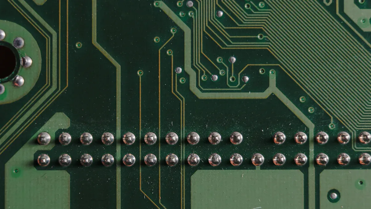
Through-hole vias are holes that connect the top and bottom layers of a PCB. They let electrical signals and heat move through the whole board. These vias are important for multi-layer PCB designs that need to be strong and reliable.
To make through-hole vias, mechanical drilling is often used. This creates holes as small as 0.006 inches wide. For even smaller holes, laser drilling is used, making sizes as tiny as 0.001 inches. Each layer needs a drill pad to stop short circuits and keep the board working properly.
Aspect | Description |
|---|---|
Definition | Links the top and bottom layers for signals and heat. |
Via Size Consideration | Depends on board thickness and aspect ratio. |
Signal Integrity Issue | Unused barrels can cause issues but fixed by back drilling. |
Characteristics of Through-Hole Vias
Through-hole vias have features that make them strong and dependable. They create solid mechanical bonds, which help the PCB last longer. This is useful for parts like connectors or large components that face physical stress.
These vias also work well with high-frequency signals. They keep impedance steady and reduce signal loss. For example, through-hole vias are often designed with 50 Ohms impedance for smooth signal flow. The size of the ring around the via helps handle drilling errors, making the board more reliable.
Key features of through-hole vias:
Strong support for parts under stress.
Good at carrying heat and electricity.
Handles high-frequency signals with controlled impedance.
Stays reliable even with physical pressure.
A common example is the 20/10mil via. The hole is 10mil wide, with a 20mil pad and a 5mil ring.
Advantages of Through-Hole Vias
Through-hole vias have many benefits, making them a favorite in PCB design. Their strong structure keeps parts firmly attached, even in tough conditions. This makes them great for uses like cars, planes, and industrial machines.
Durability
Through-hole vias are strong and handle vibration or frequent use well.High Reliability
They provide steady electrical connections, lowering the chance of failure.Thermal Management
These vias help remove heat, which is important for high-power devices.Ease of Inspection
Since they are visible, it’s easy to check and test them during production.
Through-hole vias are still a trusted choice for traditional PCB designs where strength and performance matter most.
Disadvantages of Through-Hole Vias
Through-hole vias have some downsides that make them less useful for modern PCB designs. These issues can affect how well your circuit board works, especially in small and crowded layouts.
Space Constraints: Through-hole vias take up more room because they are bigger. This makes them less useful for designs with many parts. SMT is better for saving space in tight layouts.
Not Ideal for Modern Designs: Devices like smartphones need smaller and smarter PCBs. Through-hole vias are too big and don’t fit these needs well.
Lower Processing Power: SMT allows more parts in small spaces, boosting power. Through-hole vias need more room, which limits their use in advanced designs.
Harder Routing: Bigger through-hole vias make routing harder in multi-layer PCBs. This adds time and cost to the design process.
Tip: For compact and high-performance designs, try blind or buried vias. They save space and improve signal quality.
Applications of Through-Hole Vias in Traditional PCB Designs
Through-hole vias are still helpful in older PCB designs where strength and reliability matter most. They work well in areas needing strong connections and good heat control. Here are some common uses:
Application Area | Description |
|---|---|
Power Distribution | Big vias near high-power parts; small vias for local power. |
EMI Sensitive Areas | Ground vias around sensitive circuits; extra vias spaced evenly. |
Thermal Management | Thermal vias move heat from hot parts to cooler areas; filled with heat-conducting material. |
Component Layer | Capacitors with nearby vias connect to power and ground planes. |
Overall Layout | Via fences protect sensitive sections; separate analog and digital areas. |
Thermal Vias Case Study | 25 thermal vias dropped temperature from 125°C to 85°C; 49 vias lowered it further to 75°C. |
Through-hole vias are great for uses like factory machines, car electronics, and airplane systems. They handle high currents and remove heat well, making them perfect for power and cooling tasks. For example, thermal vias filled with special material can cool parts down a lot, helping them last longer.
Note: Use through-hole vias in older PCB designs for strong connections and heat control. They are reliable and work well over time.
Comparative Analysis of Vias
Cost Comparison of Blind, Buried, and Through-Hole Vias
When making a PCB, cost is very important. Each via type has different costs based on how it’s made and the tools needed.
Through-Hole Vias: These are the cheapest option. They use simple mechanical drilling, which is common and easy to do. If your design doesn’t need tight connections, these vias save money. But they take up more space, which can make the PCB bigger.
Blind Vias: These cost more than through-hole vias. They need special methods like laser or depth drilling. These methods connect outer layers to inner ones without going through the whole board. Even though they cost more, blind vias can reduce the number of layers, saving some money.
Buried Vias: These are the most expensive. They use a process called sequential lamination, which takes time and special tools. Buried vias are great for small, multi-layer PCBs, but their high cost makes them best for designs needing compact and high-performing boards.
Tip: For simple designs and tight budgets, use through-hole vias. For complex PCBs, compare the benefits of blind and buried vias with their costs.
Complexity in Manufacturing for Different Via Types
Making vias can be simple or hard, depending on the type. Knowing this helps you pick the right via for your PCB.
Through-Hole Vias: These are the easiest to make. The process involves drilling through the whole board and plating the holes. Most manufacturers can do this easily, making it a good choice for basic designs.
Blind Vias: These need more precision. The process drills partly into the board to link outer and inner layers. Advanced tools like lasers are often used. This makes the process harder and needs skilled workers.
Buried Vias: These are the hardest to make. They connect only inner layers, leaving outer layers untouched. Sequential lamination is used, where layers are built and drilled in steps. This process is slow and needs experts and special machines.
Note: Always check with your PCB maker to ensure they can handle the vias you need. This avoids mistakes and saves time.
Performance and Reliability of Blind, Buried, and Through-Hole Vias
How well a PCB works depends on the vias used. Each type has its own strengths and weaknesses.
Through-Hole Vias: These are strong and reliable. They work well for parts under stress, like connectors. But their bigger size can cause signal loss in high-frequency designs.
Blind Vias: These improve signals by lowering unwanted electrical effects. They are great for fast and high-frequency designs, like in phones and graphics cards. However, if made poorly, they can fail.
Buried Vias: These perform well in multi-layer PCBs. They reduce signal loss and improve control. They are reliable if made correctly, but their hidden position makes fixing them hard.
Tip: Use blind and buried vias for high-speed designs. Through-hole vias are better for strong and cost-friendly designs.
Picking the Best Via Type for a Blind Buried Hole Circuit Board
Choosing the right via type is key for good performance and cost savings. Blind, buried, and through-hole vias each have special features for different designs. To decide, think about your board's needs, manufacturing options, and budget.
1. Know Your Design Needs
Start by looking at your circuit board's design. Think about these points:
Layer Count: For multi-layer boards, buried vias connect inner layers without touching outer ones. Blind vias link outer layers to inner ones.
Space Limits: Blind and buried vias save space in tight designs by avoiding through-hole connections.
Signal Quality: High-frequency circuits work better with blind and buried vias since they reduce signal loss and interference.
Tip: Use blind vias for dense designs like smartphones. Choose buried vias for complex boards in cars or medical devices.
2. Check Manufacturing Skills
Not all manufacturers can make advanced vias. Blind and buried vias need special tools like laser drills and lamination. Before finalizing, ensure your manufacturer can handle blind buried hole circuit boards.
Via Type | Difficulty to Make | Tools Needed | Cost Level |
|---|---|---|---|
Through-Hole | Easy | Regular drilling tools | Low |
Blind | Medium | Laser or depth drills | Medium |
Buried | Hard | Sequential lamination | High |
3. Balance Cost and Benefits
Blind and buried vias improve performance but cost more. Through-hole vias are cheaper but take up more space. To decide:
Pick through-hole vias for simple, low-cost designs.
Use blind vias when space and signal quality matter most.
Choose buried vias for compact, high-performance boards where cost is less important.
4. Think About Reliability
Reliability is crucial for circuit boards. Poorly made vias can fail, especially in tough conditions. Blind and buried vias need precise work to avoid problems like weak plating. Work with a skilled manufacturer to ensure quality.
Note: Test prototypes carefully to find and fix issues before mass production.
5. Match Via Type to Use
Different uses need different vias. For example:
Consumer Electronics: Blind vias are great for small devices like phones and tablets.
Car Systems: Buried vias suit multi-layer boards in advanced driver-assistance systems (ADAS).
Industrial Machines: Through-hole vias are strong for heavy-duty equipment.
By choosing the right via type for your application, you can improve your board's performance and reliability.
Final Thought: Picking the right via type means thinking about your design, manufacturing options, and use case. Blind and buried vias are great for modern boards, while through-hole vias are reliable for older designs. Decide based on your needs to make the best choice.
Knowing how blind, buried, and through-hole vias differ is important for making a good circuit board. Blind vias join outer layers to inner ones. Buried vias connect only inner layers. Through-hole vias go through the whole board. Each type is used for different design needs. Blind and buried vias are best for small, high-performance boards. Through-hole vias are better for simple, budget-friendly boards. Picking the right via type helps improve performance, save money, and make sure your circuit board works well.
FAQ
What is the main difference between blind, buried, and through-hole vias?
Blind vias link outer layers to inner ones. Buried vias connect only inner layers and stay hidden. Through-hole vias go through the whole board. Each type fits different designs based on space, cost, and performance.
Tip: Pick vias that match your PCB's design and purpose.
Why are blind vias more costly than through-hole vias?
Blind vias need special methods like laser or depth drilling. These methods require precision and advanced tools, raising costs. Through-hole vias use simpler mechanical drilling, making them cheaper.
Can through-hole vias work in high-frequency designs?
Through-hole vias can work but may cause signal loss. Their larger size can create issues in high-frequency circuits. Blind and buried vias are better as they improve signals and reduce unwanted effects.
How do buried vias make PCBs better?
Buried vias improve performance by cutting signal loss and interference. They connect inner layers directly, making signals faster and more controlled. This is great for small, fast, multi-layer PCBs.
Can all manufacturers make blind and buried vias?
Not every manufacturer can make blind or buried vias. These need advanced tools and skilled workers. Before designing, check if your manufacturer can handle these vias.
Note: Always share your design needs clearly with your PCB maker.
See Also
Explore Cutting-Edge HDI PCB Prototyping Methods Right Now
Exploring Rogers R4350B, R4003, And R5880 For RFPCB Uses
Defining PCB Printed Circuit Boards And Their Fundamental Ideas