Blind Via Technology in Multilayer PCBs and how LT CIRCUIT optimizes space and performance
Blind via technology helps connect layers in PCBs easily.
LT CIRCUIT uses blind vias for smaller, better circuit boards.
Wiring can fit more tightly, up to 20% more wires.
More parts can fit too, up to 20% more components.
These changes help PCBs work better and save space.
This is important for advanced PCB uses.
Key Takeaways
Blind vias link just the needed layers in PCBs.
This saves space and lets us add more wires and parts.
Boards can be smaller and hold up to 20% more stuff.
Blind vias make signal paths shorter and cleaner.
This cuts down on noise and helps the board work better.
PCBs can run faster and are more reliable this way.
LT CIRCUIT uses smart blind via methods and tough materials.
They build strong, high-quality PCBs for many needs.
Their boards meet strict rules and what customers want.
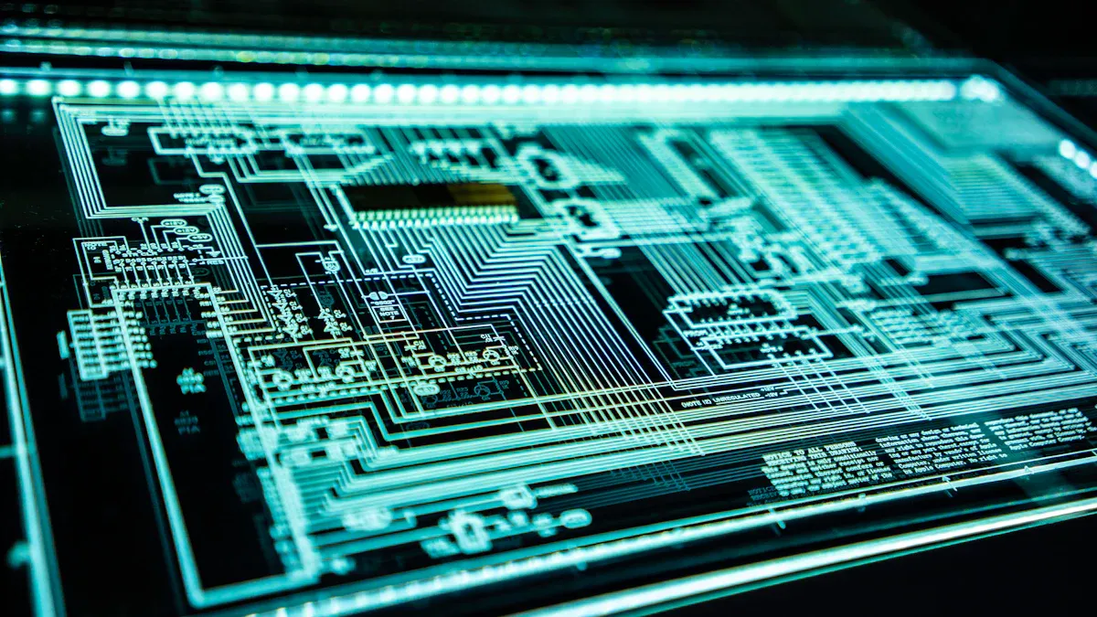
Blind Via Technology in PCB Design
What Are Blind Vias
Blind vias are important in new PCB designs.
A blind via is a small hole with metal inside.
It connects the top layer to inside layers, not all the way through.
These holes are made by drilling partway into the board.
Drills or lasers stop at a certain layer.
Copper is added to make the hole carry electricity.
A special finish keeps the board safe.
Blind vias are only on one side of the board.
This helps engineers link layers and keep the outside neat.
It lets them make small, complex boards with many parts.
Note: IPC rules say blind vias are tiny holes, 6 mils wide or less.
They connect the outside layer to an inside layer.
These rules help make sure PCBs work well and are easy to build.
Benefits for Multilayer PCBs
Blind vias give many good things to multilayer PCBs.
They only join the layers that need to be linked.
This saves space and lets more wires fit in.
Designers can put more parts and wires in a small spot.
This is needed for phones and tablets.
Blind vias can also lower the number of layers.
This makes the board thinner and lighter.
The table below shows some industry benefits:
Documented Industry Benefit | Explanation |
|---|---|
Enables HDI Designs | Lets designers put lots of parts close together. |
Increases Routing Area | Gives more room for wires on some layers. |
Reduced Layer Count | Makes routing easier and uses fewer layers. |
Improves Signal Integrity | Keeps signals clear and reduces noise. |
Potential Cost Savings | Can make boards smaller and cheaper to build. |
Blind vias help keep signals strong and clear.
Shorter paths and fewer jumps between layers lower signal loss.
Reports show blind vias keep the board’s surface clean.
This is important for fast or radio signal boards.
Blind vias let engineers use space better and add more parts.
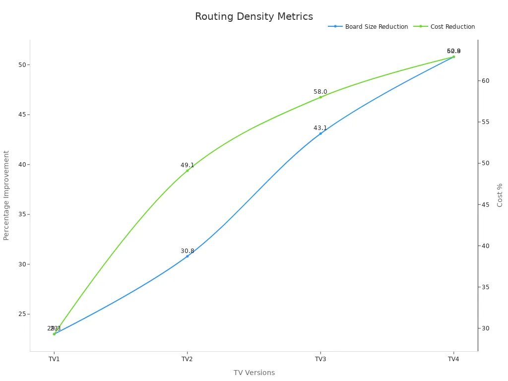
Space and Performance Optimization
Engineers use blind vias to save space and boost performance.
Blind vias let them pack more wires and parts together.
This makes boards smaller and more powerful.
Tests show blind vias with copper can fit 10% to 30% more wires.
This means more connections and parts on each layer.
Boards can be made smaller overall.
The chart below shows how blind vias cut board size and cost:
Blind vias also help signals travel better.
They make signal paths shorter and cut down on layer jumps.
Studies show the shape and size of vias matter for signal quality.
Good blind vias keep signals strong, which is key for fast data.
Tests prove blind vias help save space and improve performance.
They meet IPC rules, use fewer layers, and help with tricky parts.
Blind vias keep signals clearer than regular holes.
For example, blind vias lose about 7 dB in the 40-80 GHz range.
Regular holes lose up to 10 dB.
Blind vias work well up to 22 GHz, while regular holes work up to 15 GHz.
These numbers show blind vias are efficient and reliable.
Tip: When designing multilayer PCBs, pick the right via size and spot.
This helps save space and keeps signals strong.
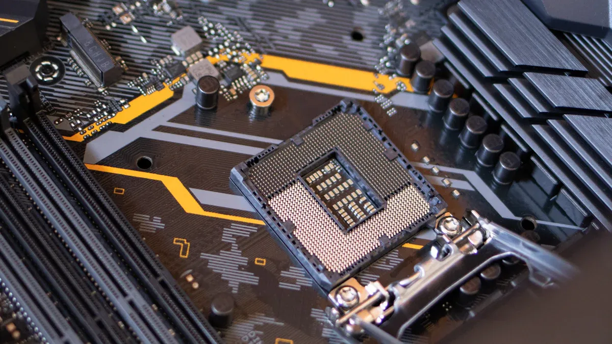
LT CIRCUIT and Advanced Blind Vias
Innovative Manufacturing
LT CIRCUIT is known for making great PCBs.
They use special ways to make boards with more parts.
Their machines drill tiny holes called blind vias.
These holes only connect the layers that need it.
This saves space and helps make tricky boards.
LT CIRCUIT picks strong materials for each board.
Thicker copper lets more electricity flow safely.
It also helps move heat away from the board.
Their boards can handle lots of power without breaking.
This makes the boards work better and last longer.
The table below shows how LT CIRCUIT’s work helps:
Metric / Test Type / Standard | Description / Purpose | Before / After or Pass Rate |
|---|---|---|
Lot Reject Rate (LRR) | Percentage of defective lots rejected | |
Fault Rate | Percentage of faulty PCBs detected | Reduced from 0.76% to a lower rate |
Maximum Current Load Capacity | Maximum safe current the PCB can carry | Improved with thicker copper layers |
Thermal Stability at Peak Power | PCB's ability to operate under high heat | Enhanced |
Heat Transfer Rate | Speed of heat dissipation | Increased |
Resistance Across Traces | Electrical resistance affecting power loss | Reduced |
Peel Strength Test | Adhesion strength of copper layers | Ensured durability |
Compliance with IPC-6012C | Copper thickness and hole quality standard | Pass rate > 99.5% |
Compliance with IPC-A-600G | Visual quality standard for PCBs | Pass rate > 99% |
Compliance with ISO 9001:2015 | Quality management certification | Ensures consistent quality |
These results show LT CIRCUIT makes fewer mistakes.
Their boards are strong and work well every time.
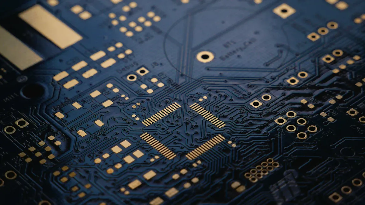
Custom PCB Solutions
LT CIRCUIT gives many choices for making PCBs.
They make boards with many layers and tiny parts.
You can pick different finishes and colors for your board.
They also check each board with special tests.
Customers like that LT CIRCUIT listens to their needs.
The company changes its work to fit each project.
Surveys show people are happy with their boards.
Many customers buy again because they trust LT CIRCUIT.
Customer happiness scores stay high.
More people order again as service gets faster.
Fewer mistakes mean more good boards.
LT CIRCUIT uses tools to watch and improve service.
LT CIRCUIT helps save space and keep signals clear.
Their engineers use blind vias to fit more parts in less space.
This is good for phones and machines that need small boards.
Quality and Reliability
LT CIRCUIT cares a lot about quality and trust.
They follow strict rules to make sure boards are good.
They test each board to find and fix problems early.
LT CIRCUIT checks every step to keep boards working right.
They use flying probe and bed-of-nails tests for this.
These tests make sure each board does what it should.
Note: LT CIRCUIT passes important tests over 99% of the time.
This means their boards last long and work well for customers.
LT CIRCUIT’s focus on quality and new ideas makes them a top choice.
They work hard so every board is strong and works great.
Blind via technology helps multilayer PCBs in many ways:
Lets engineers put parts where they need them.
Helps boards work better with less signal trouble.
LT CIRCUIT is great at using blind vias.
They help customers make small, strong circuit boards.
Think about using LT CIRCUIT for your next board project.
FAQ
Why are blind vias important in multilayer PCBs?
Blind vias link outside and inside layers.
They do not go through the whole board.
This saves space on the circuit board.
It lets more parts fit in a small area.
How do blind vias help signals and performance?
Blind vias make signal paths shorter.
Shorter paths mean less signal loss.
There is also less noise or mix-up.
This helps the board work better and faster.
What should engineers think about for saving space?
Engineers must pick the right via size.
They should also choose good spots for vias.
Good planning helps use space well.
It keeps signals strong and the board efficient.
See Also
Understanding Multilayer PCBs and Their Role in Electronics
Exploring Diverse Industry Uses for Multilayer PCBs
Challenges in Manufacturing and Prototyping Multilayer Boards