Buried Via Technology in Multilayer PCBs: Applications and Manufacturing Challenges Solved by LT CIRCUIT
Buried via technology lets you connect inner layers of a multilayer pcb without reaching the outer layers. This approach helps you build smaller, more powerful electronics. When you use buried via technology, you improve signal paths and save space. LT CIRCUIT leads the pcb industry with advanced pcb and circuit solutions.
Key Takeaways
Buried via technology connects only the inner layers of multilayer PCBs, saving space and improving signal quality for smaller, faster devices.
This technology supports high-density designs used in industries like 5G, consumer electronics, automotive, and medical devices, enabling compact and reliable products.
LT CIRCUIT solves manufacturing challenges with advanced laser drilling, precise stack-up methods, and strict quality controls to deliver high-performance, reliable PCBs.
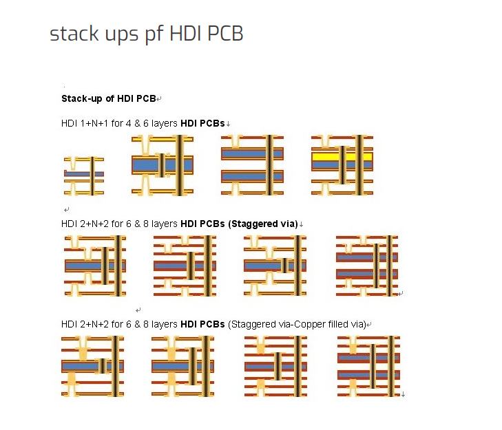
Buried Via Technology Overview
Structure and Function
Buried via technology lets you connect only the inner layers of a multi-layer pcb. You do not see these vias on the outer surfaces. Manufacturers create buried vias by drilling holes into the internal layers during the stack-up process. They fill these holes with epoxy or conductive paste and then plate them with copper. This step keeps the vias strong and reliable.
You find buried vias inside the laminated core of pcbs. The stack-up process presses copper-clad layers together, and then more layers cover the buried vias. This method keeps the outer layers free for other components and microvias. X-ray inspection tools help check the quality of buried vias, making sure every connection works as planned.
LT CIRCUIT uses advanced stack-up techniques and precise drilling to make sure every buried via meets strict standards. Their experience with high-density designs helps you get the most out of your pcb.
Benefits in HDI Multilayer PCBs
Buried via technology gives you many advantages in hdi multilayer pcbs. You can connect more circuits in a smaller space, which increases density and lets you build compact devices. This technology supports high-density interconnect designs by allowing more microvias and finer lines.
You get better signal quality because buried vias shorten the path for signals and reduce interference.
You can place more components closer together, which makes your pcb smaller and faster.
You improve thermal management since buried vias help move heat away from hot spots inside the stack-up.
Note: Industry studies show that using buried via technology in hdi multilayer pcbs can reduce board size by up to 40% compared to traditional designs. This means you can fit more features into your products without making them bigger.
LT CIRCUIT’s expertise in stack-up design and microvias ensures your pcb meets the highest density and performance needs. Their custom stack-up solutions help you achieve reliable, high-density designs for any application.
Applications and Challenges
Key Uses in Modern PCBs
You see buried via technology in many types of modern electronics. This technology helps you build smaller, faster, and more reliable devices. When you use buried vias in your pcb designs, you can connect internal layers without using up space on the outer layers. This method lets you add more microvias and components, which increases the density of your pcb.
Many industries rely on buried vias for high-performance products. For example:
5G infrastructure: You need fast and stable signals for 5G networks. Buried vias help you achieve this by shortening signal paths and improving signal quality.
Telecommunications equipment: Devices like routers and switches use buried vias to handle high-speed signals and complex routing.
Consumer electronics: Smartphones, tablets, and wearables use buried vias to fit more features into a small space. You get better performance and longer battery life.
Automotive electronics: Advanced driver assistance systems (ADAS) and infotainment systems use buried vias for reliable connections and compact designs.
Medical devices: Small medical tools need precise and reliable pcbs. Buried vias help you achieve the needed density and signal quality.
Aerospace and industrial control systems: These fields require robust and compact pcbs. Buried vias support high-density stack-up designs and improve reliability.
Market research from Verified Market Research shows that telecommunications and consumer electronics lead the way in adopting advanced pcb technologies. These sectors use buried via technology to meet the growing demand for smaller, more powerful devices.
You find buried vias in complex multilayer pcbs, sometimes with up to 30 layers and multiple stages of microvias. These designs let you route signals efficiently and keep your devices compact. Modern electronics depend on this technology to deliver high performance in a small package.
Manufacturing Challenges
When you design and build pcbs with buried vias, you face several manufacturing challenges. These challenges require advanced skills and technology to solve.
Complexity: You must manage many steps in the stack-up process. Each layer needs precise alignment, especially when you add microvias and buried vias together.
Cost: Advanced stack-up designs and extra drilling steps increase manufacturing costs. You need special equipment and skilled workers to keep quality high.
Signal integrity: You want your signals to travel without loss or interference. Buried vias help, but you must control the stack-up and via placement to keep signal quality high.
Aspect ratio: The aspect ratio is the depth of the via compared to its width. High aspect ratios make drilling and plating harder. You need to keep the aspect ratio within safe limits to avoid defects.
Precision: You must drill and plate each via with great accuracy. Even a small error can cause a weak connection or a short circuit.
Technical articles highlight these key points:
Stacked vias, including buried vias, need careful control of aspect ratio and precision during drilling and plating.
You must align each layer perfectly during the stack-up process.
Laser drilling helps you create small, accurate holes for microvias and buried vias.
Uniform copper plating is critical for strong electrical connections and thermal stability.
Advanced materials like FR-4 and polyimide improve mechanical and thermal performance.
Manufacturing complexity and cost rise with each added stack-up stage and microvia.
LT CIRCUIT addresses these challenges with advanced manufacturing processes. You benefit from their use of high-quality materials, precise laser drilling, and innovative stack-up techniques. Their team checks every pcb with strict quality controls, so you get reliable connections and high signal quality. LT CIRCUIT’s experience with complex stack-up designs and microvias ensures your pcbs meet the highest standards for density and performance.
Tip: When you choose a partner like LT CIRCUIT, you gain access to the latest stack-up innovations and manufacturing expertise. This helps you overcome the toughest challenges in modern electronics design.
LT CIRCUIT Solutions for HDI Multilayer PCBs
Advanced Manufacturing Processes
You want your pcb to deliver high performance and reliability. LT CIRCUIT uses advanced manufacturing processes to help you reach this goal. The team combines cutting-edge materials, laser drilling, and precise stack-up techniques to build complex multilayer pcbs.
Laser drilling stands out as a key technology. It creates via holes as small as 50μm, much smaller than traditional mechanical drilling. You get better position accuracy, with laser drilling reaching ±5μm. This means your buried vias line up perfectly with the stack-up, which improves signal quality and reduces scrap rates. LT CIRCUIT also uses hybrid manufacturing methods. For example, they combine mechanical pre-drilling with laser finishing. This approach gives you both cost savings and high accuracy for your buried vias.
You benefit from advanced materials like low-loss dielectrics and ceramic substrates. These materials work well with laser drilling. They help create smooth via walls and reduce chipping. LT CIRCUIT’s stack-up process uses these materials to support high-frequency signals and complex circuit designs. The team also offers multi-level cavity constructions and advanced hole fill options, such as Via-In-Pad-Plated-Over (VIPPO) and solid copper plating. These features help you achieve optimal performance in your pcb.
Tip: LT CIRCUIT’s stack-up innovations let you build custom hdi pcb solutions that meet the needs of 5G, medical, and consumer electronics.
Quality and Reliability
You need your pcb to work every time. LT CIRCUIT puts quality and reliability first in every step of the stack-up and manufacturing process. The team uses strict quality control checks, including X-ray inspection and micro-CT imaging, to make sure every buried via and stack-up layer meets high standards.
Laser drilling not only improves accuracy but also reduces defects. You see lower scrap rates and better yields. LT CIRCUIT’s use of advanced materials, such as Megtron 6 and Tachyon-100G, ensures your pcb can handle high-speed signals without loss. The stack-up process keeps signal quality high and supports robust connections between layers.
You also get the benefit of advanced plating and fill options. Solid copper plating and VIPPO help your buried vias carry signals with less resistance. The stack-up design supports thermal management, moving heat away from critical areas. This keeps your pcb stable and reliable, even in demanding environments.
Note: LT CIRCUIT’s quality checks and advanced stack-up methods help you avoid common issues like weak connections or signal loss.
Success Stories
LT CIRCUIT’s advanced stack-up and manufacturing processes have helped many customers succeed. One technical review describes a project where LT CIRCUIT used a combination of laser cutting, liquid metal spray deposition, and microvia formation to build a high-density, stretchable pcb for a cochlear implant. The process included five steps: laser-guided placement, microstructure fabrication, liquid metal spray, laser cutting, and final release from the carrier. This method produced thin, flexible circuits with multilayer vias and 40 µm wide lines.
The finished pcb went into a cochlear implant electrode array. Tests showed the stack-up and buried vias worked well, with strong electrical performance and stable signals. Micro-CT imaging confirmed the quality of the stack-up and via formation. The implant even activated auditory neurons in live tests, showing the real-world impact of LT CIRCUIT’s advanced manufacturing.
You can see similar results in other industries. LT CIRCUIT’s stack-up and laser drilling methods support high-frequency telecommunications, compact consumer electronics, and reliable automotive systems. The team’s focus on stack-up design, signal quality, and advanced materials helps you build pcbs that meet the toughest requirements.
Project Type | Stack-Up Features | Result |
|---|---|---|
Cochlear Implant | Multilayer, microvias, LM | Stable signals, robust design |
5G Telecom Board | Low-loss dielectrics, VIPPO | High signal quality |
Automotive Control | Ceramic substrate, laser | Reliable, compact pcb |
When you choose LT CIRCUIT, you get a partner who understands stack-up complexity and delivers pcbs that perform in real-world conditions.
You see buried via technology drive the future of pcb in advanced electronics. Market research shows the HDI pcb market will reach USD 21,823.6 million by 2032, fueled by buried vias. LT CIRCUIT helps you solve pcb challenges. Choose LT CIRCUIT for your next pcb project.
PCB Market | 2024 Value | 2032 Value | CAGR |
|---|---|---|---|
HDI PCB | $6,096.3M | $21,823.6M | 17.28% |
FAQ
What is a buried via in a pcb?
A buried via connects only the inner layers of a pcb. You do not see it on the outer surfaces. It helps make compact, high-density pcb designs.
Why do you need buried vias in modern pcb designs?
You use buried vias to save space and improve signal quality. They let you add more circuits and components to your pcb without making it bigger.
How does LT CIRCUIT ensure pcb quality with buried vias?
LT CIRCUIT uses advanced inspection tools and strict quality checks. You get a reliable pcb with strong connections and high performance every time.
See Also
Optimizing Space And Performance Using Blind Vias In PCBs
Exploring Diverse Industry Uses For Multilayer PCBs Today
Challenges And Processes In Manufacturing Multi-Layer Circuit Boards
Comprehensive Guide To Heavy Copper Multilayer PCB Production
Step-By-Step Overview Of The Multilayer PCB Manufacturing Process