The challenges of multiple impedance groups to PCB production capacity
Engineers have a harder job when there are many impedance groups in PCB production. They must carefully control the stack-up, materials, and process limits. This control affects how many good boards they make and how well the boards work.
Factor | Impact on PCB Manufacturing Outcomes with Multiple Impedance Groups |
|---|---|
Plating and Etching (Outer Layers) | Changes can make trace shapes different. This makes it hard to keep impedance steady. |
Inner Layer Etching | Helps keep impedance steady. It is best for important signals. |
Lamination Cycle | Changes the thickness of the dielectric. This can change reliability and impedance. |
Distance Between Signal Layer & Reference Plane | If prepreg thickness changes, impedance can change too. |
Material Properties | These affect how signals move and how easy the board is to make. |
Stackup Design Responsibility | The design engineer must pick the stackup and materials. This helps get the same results each time. |
Outer Layers vs Inner Layers | Inner layers help keep impedance steady better than outer layers. |
Multiple Impedance Groups Complexity | Needs careful process control. This stops changes and keeps yield high. |
Key Takeaways
Careful planning and clear notes help engineers handle many impedance groups. This lowers mistakes and makes PCBs work better. - Picking the best materials and watching the making steps keep impedance steady. This makes sure PCBs are strong and work well. - Working closely with makers and testing with good tools stops impedance problems. This helps make more PCBs that work right.
Impedance Groups in PCB Design

What Are Impedance Groups
Impedance groups help show how signals move on a printed circuit board. Each group has its own way that electricity acts. Engineers use these groups to guide signals and stop problems like signal loss or signal changes.
The most common impedance groups in PCB design are:
Single-Ended Impedance: This group checks impedance on one trace. Things like dielectric constant, trace width, substrate height, copper weight, and coating can change it.
Differential Impedance: This group uses two traces close together, called differential pairs. Substrate height, dielectric constant, trace width, and the space between traces matter a lot.
Coplanar Impedance: This group has a signal line with ground or power planes around it. The distance to the ground plane changes the impedance.
Each group needs careful planning to keep signals strong and clear.
Why Multiple Groups Matter
Modern PCBs often need more than one impedance group. These groups help different signals work on the same board. When engineers use many impedance groups, they face new problems.
Sudden changes in impedance can make signals bounce back. This bounce can cause ringing, overshoot, and undershoot.
Impedance mismatches often happen at vias, connector pins, branches, or splits in return planes.
These problems can make signals worse and cause more electromagnetic interference.
More impedance groups can make breaks in the path. These breaks can change signals and lower the signal-to-noise ratio.
To stop these problems, engineers must keep trace sizes the same and use good routing and termination.
Note: Keeping impedance steady and return paths smooth is very important for fast PCB performance.
Challenges of Multiple Impedance Groups
Stack-Up Complexity
Designers have a tough time with stack-up in PCBs with many impedance groups. Each group needs its own trace width, dielectric thickness, and reference plane setup. Engineers must pick the number of layers. They usually add at least one ground and one power plane. This helps keep voltage steady and noise low. Symmetrical stack-ups stop boards from bending. They also keep the dielectric thickness the same. This is important for controlled impedance.
Signal layers should have ground or power planes between them. This helps stop crosstalk, which is a problem in fast designs.
Controlled impedance needs careful math for trace width, thickness, and dielectric properties. Simulation tools help with this.
Thermal vias and materials that move heat well are added to the stack-up. This helps get rid of heat.
Vias must be used in a smart way. Stacked vias can cause stress and problems when making the board.
Putting power planes in the middle and matching them with ground planes helps. It lowers loop inductance and makes power better.
Outer layers are used for fast signals. This cuts down on via transitions and keeps signals strong.
Multi-layer PCBs with many power and ground planes need careful design. This keeps signals good and lowers EMI. PCBs with an odd number of layers cost more and bend more. This happens because of lamination tension. Bending can cause problems when making the board. Even-numbered layers help stop bending and lower the risk of defects.
Multi-layer PCBs with many impedance groups are hard to make. They take longer to build, are harder to fix, and cost more. Designers must think about cost, how well the board works, and how easy it is to make at every step.
Material and Tolerance Issues
Picking the right material and keeping tight tolerances is very important for PCBs with many impedance groups. The dielectric constant (Dk) changes impedance and how fast signals move. Lower Dk means less signal loss and less distortion. High Dk slows signals and causes more distortion.
Picking materials with the right dielectric constant is key for impedance control and good signals.
Loss tangent affects how much signal is lost. Low loss tangent materials keep signals strong.
Characteristic impedance depends on trace width, spacing, material, and stack-up.
If trace width, spacing, or layer thickness is off, impedance can change a lot. This can hurt reliability.
Stack-up and material choice must be just right to get the impedance you want.
Material properties like dielectric constant, loss tangent, CTE, thermal conductivity, and dielectric thickness matter. They affect impedance, signal quality, and board strength.
Matching CTE values in hybrid stack-ups is important. It stops stress, warping, and delamination from different expansion rates during making and use.
Careful control during lamination and drilling keeps layers lined up and impedance steady. Using even prepregs and materials with steady dielectric thickness helps keep impedance the same. Materials that move heat well help get rid of heat. This lowers thermal stress and makes the board last longer.
Routing and Density Limits
Having many impedance groups in a PCB makes routing and layer count harder. Controlled impedance routing needs certain trace widths. This limits how traces can be routed and changes routing density. Microstrip and stripline traces need different widths. This affects which layer they go on and makes routing more complex.
CAD tools let designers group nets by impedance class. This lets them set different trace widths and spacing rules. But this makes routing harder and can mean more layers.
Traces may need to be made thinner to fit tight spots, like under fine-pitch BGAs. But impedance rules limit how thin traces can be, which affects routing density.
To keep impedance right for many groups, designers add more layers. This gives each group its own reference plane and keeps traces apart. But it raises the layer count.
HDI methods like microvias and thin lines help with routing. But they often need more layers.
More impedance groups mean more layers and lower routing density because of impedance rules. The smallest trace width and spacing depend on voltage, impedance, crosstalk, how easy the board is to make, and the environment.
Factor | Condition | Minimum Spacing (relative to trace width) |
|---|---|---|
Voltage | < 50V | ~2x trace width |
Voltage | 50-150V | 3x-4x trace width |
Voltage | 150-300V | 5x-8x trace width |
Voltage | >300V | 10x+ trace width |
Impedance | 50 Ohms | 1x-2x trace width |
Impedance | 75 Ohms | 2x-3x trace width |
Impedance | 90-100 Ohms | 3x-4x trace width |
Crosstalk Prevention | Digital signals > 50MHz | >4x trace width |
Crosstalk Prevention | RF/microwave traces | >5x trace width |
Crosstalk Prevention | Sensitive analog signals | >3x trace width |
Manufacturability | >6 layer board | ~5 mils minimum spacing |
Manufacturability | 2-6 layer board | ~6 mils minimum spacing |
Manufacturability | Double-sided board | ~8 mils minimum spacing |
Manufacturability | Thick copper boards | >10 mils minimum spacing |
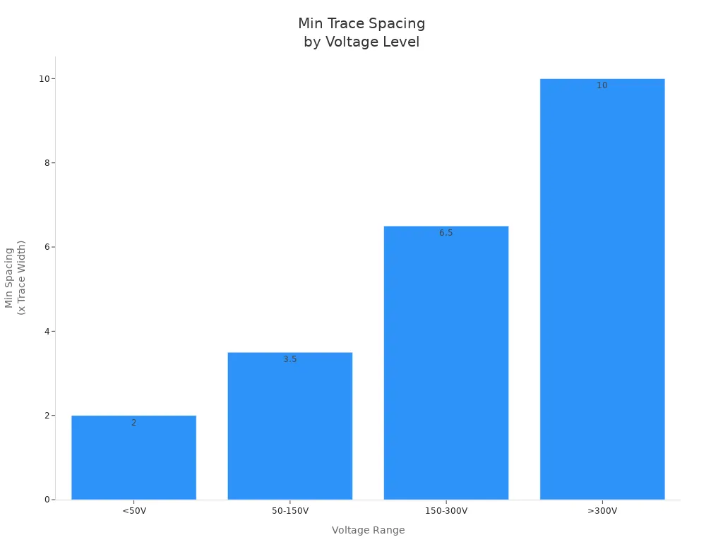
Designers must set trace width and spacing rules for each signal type, voltage, impedance, and how the board is made when working with high-density PCBs with many impedance groups.
Testing and Verification
Testing and checking PCBs with many impedance groups is hard. Impedance measurements can change a lot based on the rise time of the TDR test signal. This can make results differ by up to 4%. These changes can make good boards fail the test by mistake. Different TDR machines give different results because their edge rise times are not the same. This changes the measured impedance.
Where you measure along the trace matters. Measuring near the start is more correct. Measuring farther away adds DC resistance and makes impedance look higher.
Impedance can change along the trace and between layers. This makes testing harder and can make it tough to decide if a board is good.
These testing problems are worse for PCBs with many impedance groups. They can make you throw away good boards or keep bad ones. This hurts how many good boards you get.
Using the same test tools and ways to measure is very important. It helps keep results the same and improves yield.
Advanced testing like TDR and VNA is best for checking impedance in hard PCBs. Makers use test coupons that copy the impedance parts of the PCB. This is because testing every single impedance circuit is not possible.
For hard PCB designs with many impedance groups, advanced checks use 2D and 3D field solvers and S-parameter analysis. These tools simulate impedance and signal quality. After layout, these checks help find and fix impedance problems. Controlled impedance rules should be set in PCB CAD tools. This keeps impedance right during routing.
Solutions from LT CIRCUIT
Early Planning and Simulation
LT CIRCUIT always starts with careful planning. Their engineers use special tools like HyperLynx and Ansys SIwave. These tools help them find unwanted capacitance and inductance. They run network tests to check signal strength. EMI tests make sure the board meets rules. Thermal and mechanical tests spot heat and stress problems early.
Parasitic extraction finds hidden electrical effects.
Differential pair routing helps lower noise and crosstalk.
Careful via and part placement keeps signals strong.
Simulation feedback helps improve designs before making boards.
Planning early with these steps helps the board work well, even with many impedance groups.
Material Selection and Sourcing
LT CIRCUIT picks good materials like FR-4, Rogers RO4350B, and Isola FR408HR. These materials have steady electrical properties and are strong. Their supply chain is fast, with lead times as short as 2-5 days. Engineers can pick custom layer counts, solder mask colors, and thicknesses.
This careful picking helps with high-density interconnects and small parts. Technical support helps customers choose the best materials for their needs.
Process Control and Quality
LT CIRCUIT keeps tight tolerances when making boards. They use laser drilling for microvias and electroless plating for even copper. Nitrogen ovens help make strong solder joints. Testing uses Time Domain Reflectometry, Scanning Electron Microscopy, and thermal cycling.
Automated optical checks and X-rays find defects early.
Following IPC-6012 Class 3 and ISO 9001 keeps quality high.
Real-time checks and advanced testers keep yields high.
Their process meets or beats industry standards for PCBs with many impedance groups.
Collaboration and Communication
LT CIRCUIT works with customers from the start. They match material thickness and copper height to the design. Clear rules for each layer stop confusion. Engineers use simulation and testing tools to check impedance before making boards.
Working together early matches design and making.
Keeping trace widths and spacing the same keeps impedance steady.
Expert help solves problems fast.
This teamwork lowers the risk of impedance mismatches and helps make good PCBs.
Best Practices for Multiple Impedance Groups
Documentation Essentials
Good documentation is very important for making PCBs with many impedance groups. Engineers should do these things:
Make a clear impedance table. It should show trace width, spacing, copper weight, layer name, and target impedance for each group.
Do not use unclear notes. Say exactly which layers and trace shapes need impedance control.
Only list layers that use the given trace shapes. This stops confusion.
Say if you can change the stack-up to reach impedance goals.
Write down impedance tolerances, usually ±10%. Say if you need tighter tolerances.
Make sure stack-up pictures and notes match each other.
Use official drawings or README files to write down all details, like material types and how many layers there are.
Good documentation helps makers understand what you want. It helps control impedance and lowers mistakes. It also helps check quality and find problems early.
Communication with Fabricators
Talking clearly with fabricators makes sure they know the impedance needs. PCBA drawings give lots of technical details. These include board shape, stack-up, drill info, and assembly steps. These drawings help explain impedance needs and lower mistakes.
Communication Method | Description |
|---|---|
Tell the impedance, trace width, spacing, and tolerance for each layer. | |
Standard Design Data Files | Use IPC-2581, Gerber, or ODB++ files to share design and making info. |
PCB Fabrication Drawings | Add impedance tables, drill charts, and making details. |
Checking designs with fabricators helps find problems early. Fabricators can give tips to make boards easier to build and keep impedance steady.
Verification Methods
Good ways to check impedance are needed before making many boards. Time Domain Reflectometry (TDR) is great for checking impedance in fast PCBs. In-circuit testing (ICT) and flying probe testing check things like resistance and capacitance, which relate to impedance. Automated Optical Inspection (AOI) and X-ray Inspection (AXI) find outside and inside defects, but they do not check impedance.
Use TDR, ICT, and flying probe testing together for good checking.
Use AOI and AXI to find defects early.
Simulations and Smith Chart math help in design but do not replace real tests.
Using many checking methods makes sure PCBs with many impedance groups are good and work well.
Planning early, writing clear documents, and working together help teams make fewer mistakes. These steps also make the boards better and help finish them faster.
LT CIRCUIT uses special fine-line tools and careful process checks. Their skills help them make strong PCBs for hard designs.
LT CIRCUIT is known as a trusted company for advanced PCB solutions.
FAQ
What is the main risk of using multiple impedance groups in PCB design?
Using many impedance groups can cause more signal loss and interference. Careful planning and testing help lower these problems.
How does LT CIRCUIT ensure quality for complex impedance requirements?
LT CIRCUIT uses special simulation tools and strict process checks. They also test boards in real time. These steps help keep impedance steady and make boards more reliable.
Can engineers request custom impedance values for each group?
Option | Availability |
|---|---|
Custom Values | ✅ Yes |
Standard Values | ✅ Yes |
Engineers can ask for custom impedance values for each group. LT CIRCUIT lets you pick standard or custom options.
See Also
Essential Steps For Managing Multi-Impedance In PCB Fabrication
Enhancing Signal Integrity Through Effective Impedance Control Methods
Challenges Faced During Prototyping And Production Of Multi-Layer PCBs
Overcoming Manufacturing Issues With High TG FR4 PCBs In Industry
Typical PCB Design Issues And Fixes For SMT Processing Standards