How to choose the right PCB and EMS solutions for smart home products

Your smart lock drops its Wi-Fi connection at the front door. Your motion sensor burns through batteries in weeks. These failures rarely come from bad firmware alone. They trace back to early decisions about the PCB and EMS solutions behind the product.
You can choose the right PCB and EMS solutions by starting with product requirements. From there, you evaluate PCB design, screen EMS providers, plan costs, and confirm compliance testing. Each step shapes wireless range, power draw, and long-term reliability.
This guide gives product managers and engineers a practical path for selecting partners for smart home products. You will learn to compare capabilities, not just quotes, and build smart home devices that hold up in real homes.
Key Takeaways
Start with product requirements before you choose any PCB or EMS partner.
Match the wireless protocol to the device's power, range, and battery needs.
Design the PCB with proper layer count, impedance, and manufacturability in mind.
Screen EMS providers for certifications, technical depth, and supply chain strength.
Compare total cost of ownership instead of just unit price.
Plan FCC, CE, and regional compliance testing from day one.
Run temperature, humidity, and reliability tests on production-representative units.
Define Requirements for Smart Home PCB and EMS Solutions
Smart home products span lighting, thermostats, locks, cameras, doorbells, sensors, plugs, and voice assistants. Each type places different demands on the board. Start with product requirements before vendor evaluation. This discipline makes smart home pcb and ems solutions measurable.
Confirm Wireless Protocols and Connectivity Standards
The wireless standard for smart home lighting might be Zigbee or Thread. A wireless standard for smart home lighting that relies on Wi-Fi changes antenna design, PCB stackup, and certification. Compare Wi-Fi, BLE, Zigbee, Thread, and Matter before you start pcb design. Wi-Fi offers bandwidth but draws power; BLE suits battery sensors; Zigbee and Thread support low-power mesh; Matter adds interoperability but needs certification tests. Each protocol affects trace spacing, impedance control, and antenna clearance. Match wireless and iot components to the protocol, then plan Wi-Fi conducted and radiated tests or BLE range checks. Lock the protocol before any pcb and ems selection begins.
The protocol defines your certification path, so document firmware, antenna type, and output power early.
Set Power, Size, and Environmental Constraints
Smart home devices divide into power classes. Motion, climate, leak, and air sensors run on coin or AA cells for years using Zigbee, Thread, or BLE. Smart locks need a low-battery fallback such as a physical key, PIN, or Bluetooth. Cameras connect to mains power or use rechargeable batteries. Outdoor smart home devices face moisture and temperature swings. Many video doorbells operate from -4°F to 122°F. Battery life drops in extreme temperatures, and charging stops below freezing. Reliable smart home pcbs use conformal coatings. Smart-home PCBA designs often target a 96% moisture-resistance metric and 98% thermal stability.
Size also drives pcb layer count for a smart thermostat. A compact wall thermostat may need four or six layers for display, radio, and sensor inputs. Document enclosure dimensions, temperature, and battery life. These constraints determine your complete pcb design. Power budgets for smart home products include sleep current and peak transmit current. These smart home devices also need enclosure-specific testing.
Build an RFQ Checklist for PCB and EMS Solutions
A complete RFQ makes pcb and ems solutions comparable. Include project name, revision, owner, prototype volumes, and production volumes. Attach an Excel BOM with manufacturer part numbers and alternates for passives. Send Gerber files and fab drawings with board size, thickness, layer count, part number, and revision. Name acceptance criteria, quality standards, and test requirements. Specify AOI, X-ray, or flying probe inspection. Define lot traceability and quality records. Add packaging, delivery dates, NDA, and quote validity. Request itemized NRE pricing. State special handling such as conformal coating, RoHS, ITAR, or EAR.
This checklist lets every EMS provider quote the same scope. It exposes gaps in capability. This creates a repeatable process for smart home product development. These smart home products demand consistent quality. The right EMS partner emerges when requirements drive the conversation.
Evaluate PCB Design and Fabrication Capabilities
Smart home devices pack radios, sensors, and power circuits into small enclosures. A video doorbell or smart thermostat may need a compact, high-density board that preserves wireless performance. Multi-layer and flexible circuits help you fit these components without sacrificing signal integrity. Evaluate your manufacturer against practical criteria before you commit.
Select Materials and Layer Counts for RF Performance
Your pcb layer count for a smart thermostat depends on the display, radio, and sensor inputs. A well-routed 4-layer board often handles consumer and IoT applications, including RF modules and gateways. More layers add stackup height and require extra lamination cycles. Each added layer raises cost. The true cost driver is lamination cycles, not layer count alone. A 4-layer board with one lamination cycle costs far less than any build needing sequential lamination.
Signal integrity depends on reference plane placement. Place each signal layer one dielectric layer away from a ground plane. A continuous ground plane directly beneath high-speed signal layers reduces loop area and provides a low-impedance return path. Plane slots and voids can degrade impedance by 5 to 15 percent. For RF designs, use lower-loss laminates and tighter dielectric control. Impedance control requires consistent layer thickness and the correct dielectric constant. Standard FR-4 has a Dk of approximately 4.2. Target 50 ohm single-ended or 100 ohm differential impedance. A hybrid stackup can apply low-Dk material only to selected layers for RF and high-speed circuits.
Flexible circuits add another dimension. Define rigid and flex regions and bend radius early in pcb design. For dynamic applications, bend radius should be 100 times the finished board thickness. Insert circular cutouts with radii greater than 30 mil in bend regions without traces to increase flexibility. Avoid plated through holes and components in bend areas. Place PTH at least 20 mil away. Follow IPC-2223 for sectional design and IPC-6013 for flexible board specifications.
Use Design for Manufacturing and Assembly Rules
DFM rules protect yield in high-density pcb assembly. Via-in-pad plated-over structures need planar surfaces. Pad surface irregularity causes soldering defects because solder paste volume becomes less predictable. Non-planar pads contribute to head-in-pillow risk and inconsistent joint formation. Planarization after filling and capping blends the via area into the surrounding pad.
DFM Rule Area | Critical Guideline |
|---|---|
Via size | Via diameter typically 0.2 to 0.3 mm |
Pad dimensions | Pad at least 0.1 to 0.15 mm larger than via diameter on all sides |
Via filling | Conductive copper for thermal conductivity, or non-conductive epoxy to prevent solder wicking |
Solder mask tenting | Tenting reduces solder wicking; filled vias are preferred in high-density designs |
Adjacent via clearance | Keep at least 0.1 mm clearance between adjacent vias |
Minimum solder mask web distance is typically 4 to 5 mil. Verify fabricator capability before finalizing via placement. In high-density BGA layouts, vias may need to be tented together so solder mask openings merge into one continuous area. Document tenting requirements explicitly in fabrication notes. An example assembly note reads: all vias 12 mil or smaller to be tented both sides, except vias in thermal pads where only the bottom is tented.
Validate Prototype Support and DFM Feedback
Prototype support separates capable manufacturers from order takers. Quick-turn services complete urgent prototype assembly in approximately 24 hours. Most fast-turn projects ship in two to three days. DFM feedback gives your team actionable recommendations for manufacturability. This feedback directly affects turnaround speed, cost, quality, and yield.
Iterative DFM analysis cuts design iterations. One electronics case used AI-powered DFM to reduce iterations by 40 percent and shorten time-to-market by two months. A medical-device company cut defect rates by 60 percent after applying DFM. Pilot-run production support puts engineers on the factory floor during first runs. They watch assembly, measure quality, and fix issues the same day. This reduces early defect rates and stabilizes unit cost.
Supplier coordination matters for connected hardware such as an IoT gateway with radio, processor, power supply, and case. Keeping multiple suppliers aligned avoids line stops and batch variation. DFM and DFA choices such as fewer parts, fewer screws, and clear markings help workers assemble consistently. Structured quality checks keep feedback active after each pilot run. Choose an ems partner who provides design validation and manufacturing recommendations, not just fabrication. The right ems provider treats prototype pcb design as a collaborative engineering phase. This approach builds reliability into smart home products from the first build.
Select an Electronic Manufacturing Service Partner
Price alone cannot tell you whether an electronic manufacturing service will deliver boards that survive years in a real home. You need to evaluate industry experience, service awareness, and the ability to handle complex smart home PCBA requirements. A low quote from an inexperienced contract manufacturer often hides rework costs, missed deadlines, and field failures. The right ems partner brings engineering depth, not just capacity.
Verify Certifications and Technical Capabilities
Start with certifications. They prove that an ems provider follows recognized processes for quality and regulatory compliance. Ask every candidate for current certificates, not just claims.
Certification | Purpose |
|---|---|
ISO 9001:2015 | General Quality Management |
ISO 13485:2016 | Medical Devices |
AS9100D | Aerospace Compliance |
ITAR Registered | Secure U.S. Defense Manufacturing |
IPC 610 & J-STD-001 | Workmanship Standards |
RoHS/Lead-Free | Environmental Compliance |
ANSI/ESD S20.20 | ESD Protection |
SMTA Member | Industry Collaboration |
Beyond paper credentials, probe technical depth. Ask whether their SMT lines can place BGA and fine-pitch components and whether equipment can be programmed for a full component array. Confirm through-hole support for RF shields, connectors, transformers, and heatsinks. For conformal coating, ask which chemistries they offer — acrylic, silicone, urethane, or parylene — and how those match your operating environment. Application methods matter too: spray, dip, or selective robotic coating. Ask what IP rating the coating can achieve with enclosure sealing and whether the coating is dielectric with high dielectric strength above 20 kV/mm. RF testing deserves its own questions. A capable ems provider should confirm controlled impedance PCB handling and grounding practices that preserve signal integrity through assembly.
Communication devices involve RF design considerations and impedance control. Our controlled impedance PCB handling and grounding practices preserve signal integrity through the assembly process. Preserves RF performance.
Providers such as Flex, Vexos, and Benchmark Electronics are often cited among strong PCB assembly manufacturers for smart home products. The final choice must still align with your product's specific RF, volume, and compliance needs. An experienced pcb and ems provider will answer these questions with specifics, not generalities.
Review Supply Chain and Component Sourcing
Component shortages can halt production long before quality issues appear. A trustworthy ems partner manages sourcing risk proactively. Select components during the schematic phase that are neither obsolete nor nearing end-of-life. Verify status on manufacturer and distributor sites. Prefer newer parts, check lead times, and prioritize reputable manufacturers. After finalizing schematics, build the BOM and send it to the assembler for verification. Confirm component availability before proceeding to board assembly.
Choose alternate or backup components and common package sizes such as SOIC-8, SOT23, and TSSOP so substitutes can be found if parts go out of stock. Stay open to adjusting part values when feasible. Consider minor redesigns to achieve long-term fabrication goals. Your BOM should include an Approved Vendor List with every authorized manufacturer and distributor, alternate part numbers for critical parts, current lead times, lifecycle status per line item, and sourcing notes that preserve context for future revisions.
Lifecycle Stage | What It Means | Sourcing Action |
|---|---|---|
Active / Introduction | Manufacturer is producing and promoting the part | Safe to design in; monitor the roadmap |
Mature | Production continues, but marketing focus has shifted | Confirm long-term availability before a new design |
Not Recommended for New Designs (NRND) | Manufacturer fills existing orders but discourages new use | Avoid for new designs; identify a second source |
End-of-Life (EOL) Notice | Manufacturer announces a final order date, typically 6 to 18 months out | Place a last-time buy or qualify a replacement |
Obsolete | Manufacturer no longer produces or supports the part | Source vetted excess inventory or move to an alternate |
A medical device client had been in stable production for three years when a routine BOM review revealed their main FPGA was already in last-time-buy status. The end-of-life notice had been issued four months earlier but was missed by the engineering team, leaving only five weeks before the deadline. The contract manufacturer immediately sourced 18 months of supply and simultaneously began qualifying an alternate FPGA. Without this catch, production would have halted within six months. The monitoring effort costs roughly two hours of engineering time per customer per quarter, a trivial investment compared to a catastrophic production halt.
Never design in a component already listed as Decline or NRND. Always add secondary and tertiary approved parts to the initial AVL. Standardize passive components across all product lines to maximize buying power. Require at least two approved manufacturer part numbers for every critical IC on the BOM before approving the final prototype. Adopt the DMSMS framework, identifying alternate parts during the initial design phase rather than waiting for an emergency.
Assess Testing, Quality, and Traceability
Testing separates a reliable contract manufacturer from one that ships and hopes. PCB testing methods are categorized by test coverage, equipment, and manufacturing stage. In-circuit testing verifies individual component electrical functionality using probes contacting dedicated test points. It suits high-volume manufacturing and detects opens, shorts, incorrect values, and missing parts. Flying probe testing uses programmable robotic probes instead of fixed fixtures. It suits low-to-medium volume or prototype validation and measures continuity, resistance, capacitance, and diode characteristics. Automated optical inspection uses high-resolution cameras and image processing to detect surface-level defects like solder bridges, missing components, and incorrect polarity. It applies after paste application, placement, and reflow. Solder paste inspection targets solder deposit volume, area, and alignment before component mounting.
For ems providers, integrating testing into the broader workflow is essential. Testing should align with pcb design, assembly, and quality assurance. Design for testing principles must be implemented early in PCB layout for compatibility with ICT, flying probe, and functional test equipment. Synchronization between testing and inspection, such as combining AOI with electrical testing, enhances defect detection and lowers false positives. Seamless integration of testing systems with manufacturing execution systems enables real-time data collection, traceability, and closed-loop quality control.
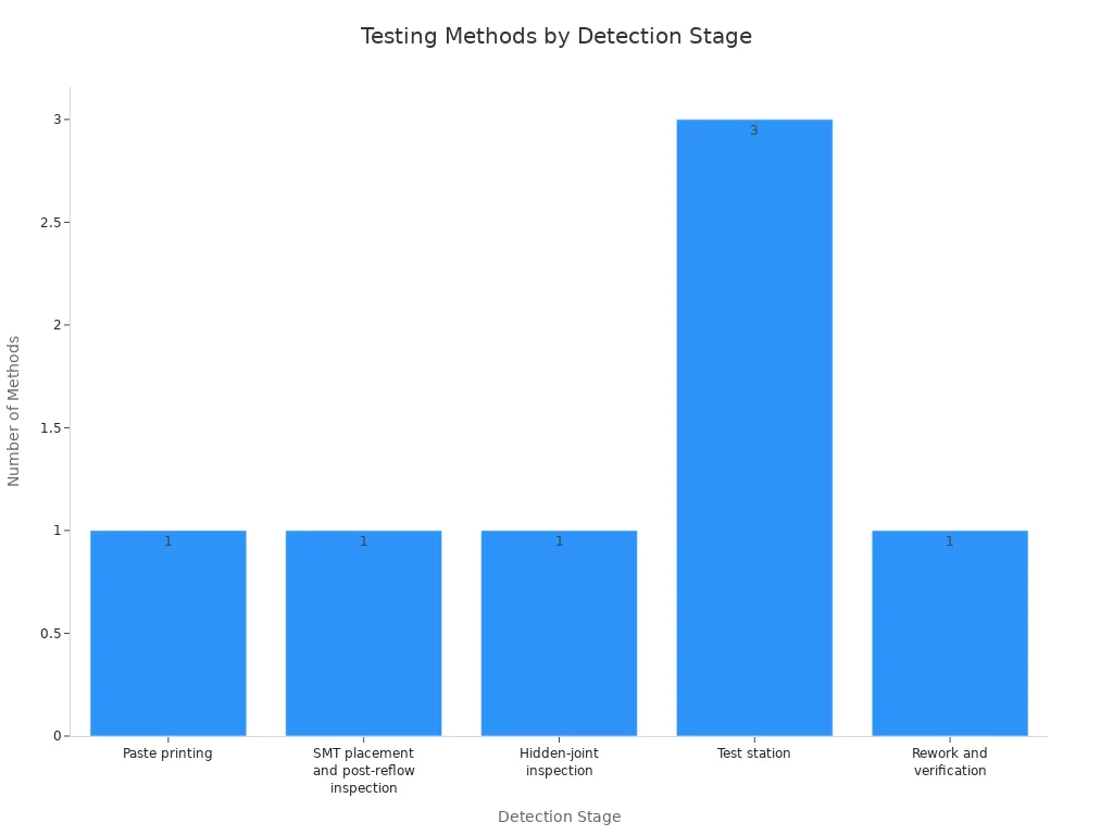
Testing/Inspection Method | Data Source | Detection Stage | Traceability Record Fields |
|---|---|---|---|
Solder Paste Inspection (SPI) | SPI result | Paste printing | SPI trend sheet with affected pads, process adjustment reason |
Automated Optical Inspection (AOI) | AOI result and placement data | SMT placement and post-reflow inspection | AOI image set with defect code and board ID |
X-Ray Inspection | X-Ray result | Hidden-joint inspection | X-Ray image set with package ID and finding code |
In-Circuit Test (ICT) | ICT result | Test station | Failure list with board ID and failed net |
Flying Probe Test | Flying probe result | Test station | Failure list with board ID and failed net |
Functional Test (FCT) | FCT result | Test station | Failure list with board ID and failed function |
Rework and Retest | NCR, repair action, retest result | Rework and verification | Closed-loop NCR summary with repair pattern and retest outcome |
Key traceability fields for inspection and testing during release check include board or lot identifier, image identifier, finding, pass or fail status, retest flag, NCR, repair action, and verification result. High-control assemblies may also use MES trend or station logs for additional verification. A contract electronics manufacturer that tracks these fields gives you a defensible quality record for every smart home device you ship.
Choose the Right PCB and EMS Solutions for Cost and Scale
Unit price alone will mislead you when you choose the right pcb and ems solutions. A low quote often hides tooling, testing, shipping, rework, and component risk. Calculate total cost of ownership before you sign with any ems provider.
Compare Total Cost of Ownership with Your EMS Provider
TCO spans five categories. Acquisition costs cover component sourcing, tooling, stencils, custom fixtures, assembly labor, and inbound freight. Operating costs include engineering support, design verification, electrical and mechanical testing, compliance documentation, and quality assurance. Supply chain costs add shipping, customs duties, tariffs, lead time variability, and inventory carrying costs. Quality and warranty costs capture returns, repairs, warranty claims, and compliance failure remediation. End-of-life costs include obsolescence management, e-waste disposal, and reverse logistics.
TCO Category | Components for EMS Comparison |
|---|---|
Acquisition Costs | Component sourcing, tooling, stencils, fixtures, assembly labor, inbound freight |
Operating Costs | Engineering support, design verification, testing, compliance documentation, quality assurance |
Supply Chain Costs | Shipping, customs duties, tariffs, lead time variability, inventory storage |
Quality and Warranty Costs | Returns, repairs, warranty claims, compliance failure remediation |
End-of-Life Costs | Obsolescence management, e-waste disposal, reverse logistics |
The TCO formula is: TCO = Acquisition Cost + Operation Cost + Maintenance + End-of-Life Disposal + Risk Factors. An ems partner with strong process controls reduces returns and warranty claims over the product lifetime. Automated optical inspection catches soldering defects early and prevents costly rework. In-circuit testing verifies electrical performance before final assembly. Advanced forecasting tools enable leaner inventory and fewer last-minute spot buys. Integrated logistics and just-in-time models cut freight expenses. Compare offshore and local ems providers on shipping predictability, tariff risk, communication delays, and rework costs. A local contract manufacturer offers faster response and lower recall exposure.
Evaluate Production Ramp and Capacity Flexibility
Smart home products often launch with seasonal demand spikes. A contract manufacturer must scale from prototype to mass production without quality loss. Ask each ems provider about surge capacity, line changeover speed, and workforce scalability. A contract manufacturer with flexible SMT lines can absorb a holiday launch spike. Confirm your ems partner can add shifts or duplicate lines during peak months. Capacity flexibility protects your launch window.
Plan Lead Times and Inventory Strategies
Lead-time variability is a common supply-chain risk. Safety stock protects production from worst-case demand and supplier delays. The formula is: Safety Stock = (Maximum Daily Usage × Maximum Lead Time) - (Average Daily Usage × Average Lead Time). Apply this to long-lead-time PCBs and components.
Safety stock is an extra buffer of critical components kept to protect against supply-chain variability and unexpected demand.
A hybrid approach uses just-in-time for standard, predictable components while keeping safety stock for long-lead-time or critical parts. Pre-stocking long-lead-time components and PCB assemblies acts as buffer stock. Scheduled releases and JIT fulfillment release inventory according to actual demand. A stocking agreement tailored to usage can adjust for demand changes. This mirrors a supplier-managed inventory relationship. Your ems provider should set safety stock and production order quantities with an MRP/ERP system to avoid stock-outs and minimize downtime. These strategies keep smart home devices supplied through seasonal peaks.
Ensure Compliance, Testing, and Reliability
Compliance failures delay launches and damage reputations. You must plan certifications, validate RF performance, and prove reliability before shipping smart home products at scale.
Plan FCC, CE, and Regional Certifications Early
Certification belongs in your schedule from day one. The FCC governs radio emissions in the United States, CE marking covers the European Union, and other regions add their own rules. Each market demands different documentation, test labs, and timelines. You should budget weeks for testing and possible retests.
Assign one owner for certification changes. A component swap or PCB design revision after launch can void FCC, CE, or UL status. That owner tracks every engineering change and flags anything touching the radio, power supply, or enclosure. This discipline protects your quality standards and regulatory requirements across the product lifecycle. Your contract manufacturer should support this process with documentation and change notifications.
Validate Antenna and RF Performance in Final Layouts
Simulations cannot perfectly predict real-world antenna behavior, especially in final integrated layouts. You need hardware testing to confirm performance. Anechoic chambers provide an environment free from echoes and external radiated signals. This isolation enables accurate measurement of how an antenna radiates energy in desired and undesired directions.
Anechoic chambers are shielded enclosures with absorptive interiors. They isolate antennas from external interference, noise, and nearby reflecting objects. Testing in this environment validates radiation pattern behavior, gain, and efficiency under strict conditions. The test method you choose depends on the antenna's operating frequency and electrical size. Common approaches include far-field illumination, near-field measurements, and compact range measurements. Each method suits different validation goals for your smart home devices.
Run Temperature Cycling and Environmental Tests
Smart home devices live in unconditioned spaces. A doorbell camera faces summer heat and winter cold. A leak sensor sits in a damp basement for years. You must test reliability against temperature, humidity, ESD, and power integrity. Temperature cycling exposes solder joint fatigue and material stress. Humidity testing reveals corrosion risks and coating failures. ESD testing confirms your PCB design survives static discharge during handling and use.
Power integrity testing matters because smart home products often remain powered for years. Voltage sags, brownouts, and surge events can degrade components over time. Your contract manufacturer should run these tests on production-representative units, not just engineering samples. This approach builds reliability into every unit you ship. A contract manufacturer with strong quality processes will document results and flag failures before they reach customers.
You now have a clear path to choose the right pcb and ems solutions. Start with requirements for your smart home products. Evaluate pcb design for wireless performance. Select an ems partner with strong certifications and supply chain depth. Balance cost with scale and compliance.
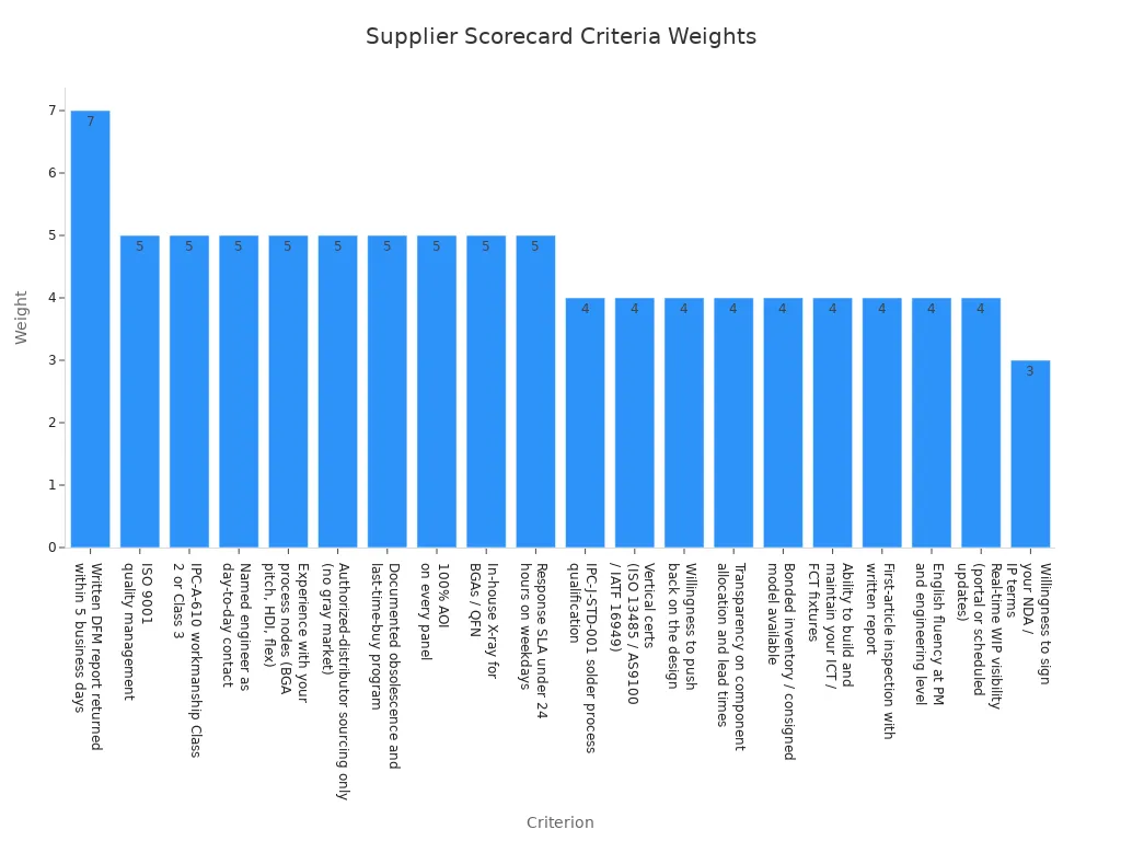
The best long-term ems partner is not always the lowest quote. Look for design feedback, consistent quality, and production flexibility. Turn these sections into a supplier scorecard, then send a prototype RFQ to at least two ems providers.
This approach strengthens smart home product development. It also helps you ship smart home devices that last.
FAQ
Which wireless protocol should I choose first?
Pick the protocol before any board layout work begins. Wi-Fi delivers bandwidth at a power cost. BLE suits battery sensors. Zigbee and Thread support low-power mesh networks. Matter adds interoperability but demands certification testing. Your choice sets antenna design, stackup, and the certification path.
How many PCB layers does a smart thermostat need?
A well-routed 4-layer board often handles consumer and IoT designs, including RF modules and gateways. Compact thermostats with a display, radio, and sensor inputs may need four or six layers. Remember that lamination cycles drive cost more than layer count alone.
What impedance should I target for RF traces?
Target 50 ohm single-ended or 100 ohm differential impedance. Standard FR-4 has a dielectric constant near 4.2. Place each signal layer one dielectric layer away from a ground plane. Plane slots and voids can degrade impedance by 5 to 15 percent.
How do I screen an EMS provider beyond price?
Ask for current certificates such as ISO 9001:2015, IPC-A-610, and J-STD-001. Confirm BGA and fine-pitch placement, conformal coating options, and controlled impedance handling. Check supply chain depth and traceability records. A capable ems partner answers with specifics, not generalities.
What drives total cost of ownership?
TCO spans acquisition, operating, supply chain, quality and warranty, and end-of-life costs. Tooling, testing, shipping, rework, and component risk all count. A low unit quote often hides these expenses. Compare providers on the full picture before you sign.
When should I start certification planning?
Start on day one. The FCC governs United States radio emissions, CE marking covers the European Union, and other regions add their own rules. Budget weeks for testing and possible retests. Assign one owner to track every engineering change touching the radio, power supply, or enclosure.
How do I protect smart home devices from environmental stress?
Test against temperature, humidity, ESD, and power integrity. Temperature cycling exposes solder joint fatigue. Humidity testing reveals corrosion and coating failures. Many video doorbells operate from -4°F to 122°F. Run these tests on production-representative units, not just engineering samples.
What inventory strategy reduces supply risk?
Use safety stock for long-lead-time parts and just-in-time for predictable components. Pre-stock critical PCB assemblies as buffer stock. A stocking agreement tailored to usage adjusts for demand changes. Your provider should set safety stock and order quantities through an MRP/ERP system.
