Circuit Board Reverse Engineering Process
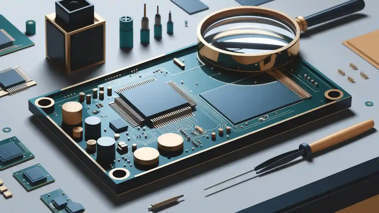
PCB reverse engineering means studying a circuit board to copy its design or learn how it works. This process is important in electronics because it helps create new ideas and fix problems. Using LT CIRCUIT’s smart tools and skills, you can make pcb reverse engineering easier and get accurate results for your work.
Key Takeaways
PCB reverse engineering helps copy and improve circuit boards. Use tools like KiCad and inspection gadgets to collect key details.
Always follow rules and laws when reverse engineering. Respect original work and use it for learning or creating new ideas.
Write down everything during the reverse engineering process. Keep notes to stay accurate and find parts more easily later.
Understanding PCB Reverse Engineering
What Is PCB Reverse Engineering?
PCB reverse engineering means studying a circuit board to learn its design. This includes looking at its parts, connections, and layout. The goal is to recreate its plan or make it better. Tools like inspection devices, testing equipment, and software like KiCad are often used. These tools help gather details about how the board works.
This process is very important in electronics today. The demand for PCB reverse engineering is growing fast. Technology improvements and its use in many industries drive this growth. Companies, schools, and chip makers depend on it to meet their needs. Regions like the Americas and Asia-Pacific lead in using this method due to innovation.
Why Is PCB Reverse Engineering Performed?
There are many reasons to reverse engineer a PCB. One reason is to replace old parts in older devices. By studying the board, you can find outdated parts and swap them. Another reason is to check or improve a design. This makes sure the board works well and meets new standards.
It also helps in studying competitors' designs. By analyzing their boards, you can learn their ideas and technology. Reverse engineering is useful for teaching and research too. It helps students and researchers understand how PCBs are made and work.
Ethical and Legal Considerations
When reverse engineering, you must follow ethical and legal rules. Respect others' designs and don’t copy without permission. Laws protect original designs, and breaking them can cause problems.
Ethical use means using reverse engineering for good reasons, like learning or creating. It should not be used to copy without approval. Courses and guides teach these rules to ensure fair practices.
Step-by-Step Reverse Engineering Process
Preparation and Initial Inspection
The first step in pcb reverse engineering is preparation. Start by looking closely at the circuit board. This helps you understand its parts and layout. Collect all needed details before moving ahead.
Here are some methods to use during this step:
Inspection Technique | Description |
|---|---|
Check components | Note details like location, size, and heat levels. |
Pre-scan | |
Remove parts | Take out bigger parts first, then scan again at 600dpi. |
Clean surface | Clean the board for clear views of labels and models. |
Also, take clear pictures of both sides of the board. Use a good camera or scanner with bright lighting. A dark background helps make copper lines easier to see.
Schematic Diagram Generation
After inspection, create the schematic diagram. This shows how the pcb layout connects its parts.
Steps to make the schematic:
Take Photos: Capture clear, high-quality images of the PCB.
Edit Images: Use software to highlight key features in the photos.
Build Layout: Create a 3D model to study circuits and signals.
Draw Schematic: Make a 2D diagram showing parts and connections.
Tools like AutoTrace or Target3001! can help. They turn layouts into schematics and organize parts logically.
Layout Reconstruction
Rebuilding the pcb layout is an important step. Study the board’s design and recreate it digitally. This often includes delayering, where you separate the board’s layers to see inside.
Steps for layout reconstruction:
Scan each layer of the PCB in high resolution.
Mark where parts, wires, and holes are located.
Use software to digitally rebuild the layout with correct sizes.
Automated tools can speed this up, but manual work may be needed for tricky designs.
Bill of Materials (BOM) Creation
The Bill of Materials (BOM) lists all the parts on the PCB. It helps you understand the design and find replacement parts.
To make the BOM:
Identify all parts like resistors, capacitors, and chips.
Write down details like part numbers and sizes.
Use software to organize this data neatly.
A good BOM makes fixing or redesigning the board much easier.
Testing and Validation
Testing and validation are the last steps. Check if the rebuilt pcb layout and schematic work properly.
During testing, look for problems like wrong connections or missing parts. Tools like multimeters and oscilloscopes help find and fix issues. Validation ensures the design works well and meets standards.
Testing includes:
Measuring electrical signals with tools.
Running simulations to predict how circuits behave.
Comparing the new design to the original PCB for accuracy.
This step ensures the reverse-engineered PCB is reliable and ready to use.
Tools and PCB Reverse Engineering Techniques
Non-Destructive Techniques
Non-destructive methods let you study a circuit board without harming it. These are great when you have only one board or need to keep it intact during the pcb reverse engineering process.
Here are some common non-destructive techniques:
X-ray Computed Tomography (X-ray CT): This uses special imaging to see inside the board. It’s helpful for boards with many layers. Experts like Asadizanjani et al. have shown its success in studying complex boards.
Automated Component Detection: Machines quickly find and identify parts on the board. This saves time and ensures accuracy.
Image Segmentation and Optical Character Recognition (OCR): These tools pull data from PCB pictures. They help you understand the design without touching the board.
Non-destructive methods are important for keeping the board safe while gathering useful details for reverse engineering.
Destructive Techniques
Destructive methods involve changing the board to see its inner structure. These methods can’t save the original board but give detailed information about its design.
Here are some common destructive techniques:
Delayering: Layers of the board are removed one at a time. Each layer is scanned to rebuild the design digitally.
Chemical Etching: Chemicals remove layers to show hidden connections. This is useful for studying buried wires and paths.
Component Removal: Parts are taken off to check their details and placement. This helps create an accurate Bill of Materials (BOM).
Destructive methods are used when non-destructive ones don’t give enough details, especially for damaged or complex boards.
Software Tools for PCB Analysis
Software tools are very helpful in pcb reverse engineering. They make tasks like creating schematics, rebuilding layouts, and checking designs easier.
Here’s a table of software types and their features:
Software Type | Examples | Features |
|---|---|---|
Schematic Capture | Altium Designer, OrCAD Capture, KiCad | Shows circuits visually, links parts, creates netlists |
PCB Layout | Altium Designer, Eagle PCB, Cadence Allegro | Places parts, manages signals, automates wiring |
Simulation | PSpice, LTspice, Simulink | Tests circuits, checks performance, analyzes heat |
Design Rule Checking (DRC) | CAM350, Valor NPI, Allegro DRC | Finds design problems, ensures rules are followed |
PCB Manufacturing | CAM350, GC-Prevue, Valor NPI | Prepares files for production, creates outputs |
Library Management | Altium ILM, Ultra Librarian, Octopart | Organizes part libraries, keeps data correct |
Signal Integrity Analysis | HyperLynx, SIWave, Cadence Allegro Sigrity | Checks signal quality, finds issues like noise and interference |
Power Integrity Analysis | PowerSI, Sigrity PowerDC, ANSYS SIwave | Studies power flow, finds voltage drops and noise |
These tools make reverse engineering faster and more accurate. For example, schematic tools show how parts connect, and simulation tools predict how circuits will work.
By using non-destructive methods, destructive techniques, and smart software, you can reverse engineer circuit boards effectively and accurately.
Applications of Circuit Board Reverse Engineering
Obsolete Component Replacement
Reverse engineering helps replace old parts on circuit boards. When devices fail due to unavailable parts, this process finds modern replacements. For example, researchers have updated old PCB designs using advanced tools. This keeps devices working without needing a full redesign. A study shows steps like collecting data, editing images, and testing circuits for single-layer PCBs. These methods solve part shortages while keeping the board's original function.
Design Validation and Improvement
Reverse engineering checks and improves PCB designs. By studying layouts and parts, you can fix mistakes and meet new standards. For example, it removes design errors, updates old semiconductors, and boosts PCB performance. The table below shows its benefits:
Evidence Description | Purpose in Design Validation and Improvement |
|---|---|
Reverse engineering can help to redesign a PCB to its rudimental design. | |
You can remove obsolete semiconductors with reverse engineering. | Ensures compliance with new environmental norms. |
Employing reverse engineering when upgrading uses existing checked components. | Saves cost and time in the redesign process. |
Improves the functionality of PCB components with a new design. | Enhances overall performance and reliability of the PCB. |
This ensures your circuit board works well with today’s technology and is more reliable.
Competitive Analysis
Reverse engineering is useful for studying competitors' designs. It helps you learn their technology and strategies. This process shows ways to innovate and improve. For example, it helps understand designs, speed up production, and find new ideas. Key points of competitive analysis include:
Trends and factors driving reverse engineering.
Market studies like PESTEL and Porter’s Five Forces.
Patent details and new technologies shaping competition.
Product life cycle stages for better understanding.
These insights help you improve designs and stay ahead in the market.
Educational and Research Purposes
Reverse engineering is great for learning and research. It teaches students and researchers how circuit boards work and how to rebuild them. By studying layouts and parts, you can learn PCB design details. It also helps create new technologies and improve old ones. Schools use it to teach skills, and researchers use it to find new solutions.
Challenges in the Reverse Engineering Process
Technical Complexity
Reverse engineering a PCB is a detailed and tricky task. It needs careful work and knowledge. You have to study the board's layers, parts, and connections. Modern designs make this harder because they are very complex. For example, multilayer boards hide important paths and holes. This makes it tough to recreate the design correctly.
Some common technical problems are:
Mistakes during testing and checking the board.
Hard steps like removing layers and making diagrams.
Worries about copying rules when hiring outside help.
The table below shows how long different PCB tasks take. It highlights how hard the process can be:
Task | Time (seconds) |
|---|---|
Automatic part placement | 15 |
Hand assembly | 125 |
Soldering | 60 |
Checking intervals | 600 |
Testing | 300 |
Fixing settings | 600 |
Control delays | 1700 |
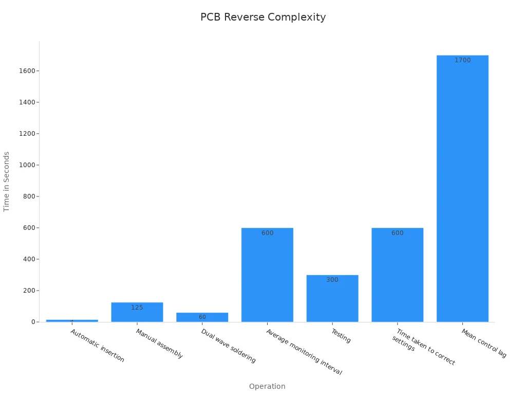
These numbers show why you need good tools and skills to handle the challenges of PCB reverse engineering.
Legal and Ethical Concerns
Reverse engineering PCBs brings up legal and moral issues. You must follow rules about copying and respect others' designs. Laws differ by country. For example, Europe allows reverse engineering for learning, but the U.S. has stricter rules under the DMCA.
The table below explains some key laws:
Law or Rule | What It Means |
|---|---|
DMCA | Limits reverse engineering, especially for software. Defines fair use. |
EU Rules | Allows reverse engineering for learning and research. Protects innovation and IP. |
Chip Protection Act | Permits reverse engineering in certain cases to create new designs. |
Kewanee Oil v. Bicron | U.S. case saying reverse engineering can help competition if done right. |
Microsoft v. Motorola | Shows how software licenses affect reverse engineering. Stresses following terms. |
You should also act responsibly. Use reverse engineering to create, not copy. Working with suppliers can help you follow rules and build trust.
Time and Resource Constraints
Reverse engineering takes a lot of time and effort. You need special tools, skilled workers, and careful study to get good results. For example, removing layers or drawing diagrams can take hours or days, depending on the board's design.
Limited money or old tools can make things harder. Manual jobs like finding parts and rebuilding layouts slow things down too. Using advanced tools and automation can save time and reduce mistakes.
By knowing these challenges, you can plan better and succeed in reverse engineering PCBs.
Best Practices for PCB Reverse Engineering
Keep Detailed Records
Writing down every step is very important in PCB reverse engineering. You should record all actions to stay accurate and organized. Good records include fixing missing labels and making a full list of parts (BOM). This helps you understand the board design and find parts faster.
Using digital files for your records is a smart choice. It lets you search through many pages easily. Marking tested points during your work saves time and avoids repeating steps. This also lowers the chance of damaging the circuit board. The table below shows helpful tips for keeping records:
Best Practice | Description |
|---|---|
Add missing labels and include a full parts list. | |
Easy Part Finding | Use digital files to search across pages quickly. |
Mark Tested Points | Highlight tested spots to save time and protect the board. |
Use LT CIRCUIT’s Advanced Tools
Using LT CIRCUIT’s tools can make reverse engineering much easier. Their smart tools help with tasks like drawing diagrams, rebuilding layouts, and checking designs. For example, their high-quality boards and testing services ensure accuracy. These tools save time and help you get better results in your projects.
Follow Ethical Rules
It’s important to follow ethical rules in PCB reverse engineering. Always respect others’ designs and don’t copy without permission. Use this process for good reasons, like learning or fixing old designs. Following these rules keeps your work legal and builds trust in the industry.
Work with Experts
Teaming up with skilled professionals can improve your reverse engineering work. Experts know a lot about tricky board designs and analysis. Working with them helps solve problems and makes your project successful. You can also learn new skills and tips by working with industry leaders.
Reverse engineering circuit boards is important in today's electronics. It lets you create, fix, and upgrade designs easily. LT CIRCUIT provides smart tools to make this task simpler and precise. Always follow rules and respect others' work to encourage new ideas in the field.
FAQ
What is the difference between destructive and non-destructive reverse engineering?
Non-destructive methods keep the PCB safe while collecting data. Destructive methods, like delayering, change the board to see inside.
Tip: Use non-destructive methods for rare or one-of-a-kind boards.
Can you reverse engineer a multilayer PCB?
Yes, multilayer PCBs can be reverse engineered. Tools like X-ray imaging and delayering help study hidden layers and connections.
Is PCB reverse engineering legal?
Reverse engineering PCBs is legal for learning, fixing, or improving designs. Do not copy patented designs without permission to follow the law.
Note: Always check your local laws before starting reverse engineering.
See Also
Explore Cutting-Edge Techniques For HDI PCB Prototyping Now
Understanding The Materials Used In Printed Circuit Boards
Exploring RF Circuit Boards: Functionality And Purpose Explained
Advantages Of LDI Exposure Machines For HDI PCB Circuit Production