Exploring Popular Stack-up Types for HDI Multilayer PCBs
HDI multilayer PCBs utilize commonly used stack-up types such as 1+N+1, 2+N+2, 3+N+3, and 4+N+4. Selecting the right setup ensures optimal performance and longevity. An effective stack-up simplifies the manufacturing process, reduces signal issues, and addresses the demands of modern electronics.
Key Takeaways
Pick the best HDI stack-up to improve design performance.
Use microvias to make routing easier and signals clearer in dense PCBs.
Choose strong materials that handle heat to last in harsh conditions.
Understanding Commonly Used Stack-up Configurations
What Makes a Stack-up "Commonly Used"?
A stack-up is "commonly used" when it works well for HDI PCBs. It must balance good performance, easy manufacturing, and low cost. Some setups are popular because they fit modern devices and stay reliable.
Here are examples of common stack-ups in HDI PCB design:
2+N+2 Structure: This has two inside layers, N outside layers, two signal layers, and one ground layer. It works best for four-layer or six-layer boards.
3+N+3 Structure: It includes three inside layers, N outside layers, three signal layers, and one ground layer. This is great for eight-layer boards.
4+N+4 Structure: This setup has four inside layers, N outside layers, four signal layers, and one ground layer. It suits ten-layer boards or more.
5+N+5 Structure: This advanced setup has five inside layers, N outside layers, five signal layers, and one ground layer. It is used for twelve-layer boards or higher.
These setups are popular because they balance space and function.
Overview of HDI Stack-up Structures
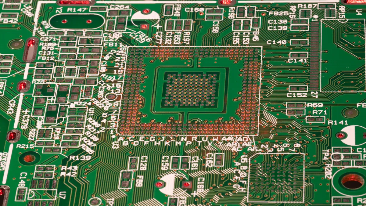
HDI stack-ups save space and keep signals strong. They use layers of metal and insulation. These designs often include microvias, buried vias, and blind vias to link layers. This helps fit more parts and boosts electrical performance.
The number of layers shows how complex the stack-up is. For example, a 2+N+2 stack-up is simpler and cheaper. A 4+N+4 stack-up is denser and better for advanced designs. Picking the right setup depends on your needs.
Role of LT CIRCUIT in HDI Stack-up Innovation
LT CIRCUIT helps improve HDI stack-up designs. They create new solutions for modern electronics. Using advanced materials and methods, LT CIRCUIT makes stack-ups that perform well and last long.
You can trust LT CIRCUIT for custom HDI PCB solutions. Their skill in multilayer and high-density designs helps them make setups that save space, keep signals strong, and manage heat better. Whether you need a 2+N+2 or 4+N+4 stack-up, LT CIRCUIT can meet your needs.
Popular HDI Stack-up Types and Their Applications
1+N+1 Stack-up: Structure and Use Cases
The 1+N+1 stack-up is a simple HDI PCB design. It has one lamination on each side of the core. This creates a total of N+2 layers. It works well for medium-complexity designs, like those with fewer BGA pins. Its basic structure makes it stable and affordable.
This stack-up is common in devices like smartphones and tablets. These devices need to be small and reliable. It’s a good choice for designs that balance performance and easy manufacturing.
Tip: Choose the 1+N+1 stack-up for simple, reliable designs with fewer layers.
2+N+2 Stack-up: Balancing Density and Performance
The 2+N+2 stack-up is more advanced than the 1+N+1. It has two laminations on each side of the core. This setup is great for HDI designs with more pins and dense BGA parts. It improves routing, which helps keep signals strong.
Metric | Description |
|---|---|
Better Signal Quality | Controls impedance and reduces signal interference. |
Higher Routing Density | Allows smaller traces and vias for more connections. |
Power Management | Uses full plane layers and multiple vias for better power flow. |
This stack-up is used in high-tech fields like computing and telecom. It supports 5G devices by improving signal quality and reliability. Its mix of density and performance makes it a favorite for modern electronics.
3+N+3 Stack-up: Advanced Routing for Complex Designs
The 3+N+3 stack-up is for more complex HDI designs. It has three laminations on each side of the core. This allows for better routing and handling of dense connections. It’s perfect for designs needing precise signal paths.
Challenge | Solution |
|---|---|
Aligning Microvias | Follow design rules for accurate via placement. |
High Aspect Ratios | Work with manufacturers to ensure proper production. |
Complex Blind Holes | Use advanced tools to manage tricky designs. |
This stack-up is used in aerospace and medical devices. These fields need small, reliable designs. It solves routing problems with advanced methods like precise microvia placement.
Note: Partner with experts like LT CIRCUIT to ensure top-quality 3+N+3 stack-ups.
4+N+4 Stack-up: High-Density Solutions for Cutting-Edge Devices
The 4+N+4 stack-up is the most advanced HDI design. It has four laminations on each side of the core. This setup is made for devices needing maximum density and speed. It’s used in high-speed computing, telecom, and IoT.
The Aruba CX 6300 Switch Series shows the power of this stack-up. It supports fast networks and high-power PoE features.
It’s also great for car electronics, like ADAS and EV systems, improving signal flow.
In aerospace, it reduces weight while staying reliable for airborne systems.
The 4+N+4 stack-up is ideal for high-tech projects needing top performance and scalability.
Tip: Use the 4+N+4 stack-up for cutting-edge designs that need high density and reliability.
Key Design Considerations for HDI Stack-ups
Signal Integrity and Layer Arrangement
Keeping signals clear is very important in HDI PCBs. You need to plan the layers carefully to avoid signal problems. Where you place signal and power layers affects how signals travel. This helps control impedance and reduces signal bouncing. Microvias and buried vias make routing easier and cut down interference, which is key for fast designs.
To keep signals strong:
Use microvias instead of through-hole vias for better routing.
Separate signal layers from power layers in your design.
Follow rules for HDI designs, like using thin lines and proper ratios.
A good stack-up keeps signals strong, especially in 5G and advanced computers.
Tip: Think about signal quality early to avoid fixing mistakes later.
Thermal Management in High-Density Designs
Good heat control keeps HDI PCBs working in hot places. Choose materials that spread heat well and add features like ground planes and thermal vias.
Here are some examples of heat control:
Car ECU: Special materials and ground planes spread heat, working at 150°C.
Space Transmitter: Ceramic boards handle space heat with strong, flexible designs.
Furnace Controller: Polyimide boards with thermal vias work near 160°C furnaces.
These examples show why picking the right materials and designs is important for heat control.
Note: Work with experts to test how your design handles heat in real life.
Material Selection for Enhanced Durability
Strong materials help HDI PCBs last longer, especially in tough industries like cars and planes. Pick materials that don’t soak up water and spread heat well.
Material Type | Heat Spread (W/m/K) | Water Absorption (%) |
|---|---|---|
Regular PCB Materials | 0.25 | ~1 |
High-Frequency Materials | 0.50 - 0.75 | <0.25 |
Testing under stress finds weak spots in your design. This makes sure your PCB works well in tough conditions.
Tip: Use stress tests to pick better materials and improve your design for long-lasting PCBs.
Picking the correct HDI stack-up improves etching and reliability. It also allows flexible routing for better designs. Think about materials and layer order for top performance. LT CIRCUIT is skilled in making HDI PCBs. They focus on design, signal quality, and heat control. Check out their custom solutions for high-density projects.
FAQ
What is the main benefit of using HDI stack-ups?
HDI stack-ups help make small designs with strong signals. They also allow more connections, perfect for modern high-tech devices.
Tip: Choose HDI stack-ups to save space and boost performance.
How do microvias help HDI PCBs work better?
Microvias cut down signal problems and improve connection paths. They link layers well, making high-density designs work smoothly.
Can LT CIRCUIT create custom HDI stack-ups?
Yes, LT CIRCUIT makes HDI stack-ups to fit your needs. They ensure great performance, long life, and easy manufacturing.
Note: Check out LT CIRCUIT's website for custom HDI PCB options.
See Also
Explore Cutting-Edge Techniques for HDI PCB Prototyping
Challenges and Processes in Multi-Layer Circuit Board Production
Advantages of LDI Exposure Machines for HDI PCB Circuits
Understanding the Production of Rigid-Flex Multilayer Circuit Boards