Comparing PCB Microsectioning Techniques for Superior Defect Detection
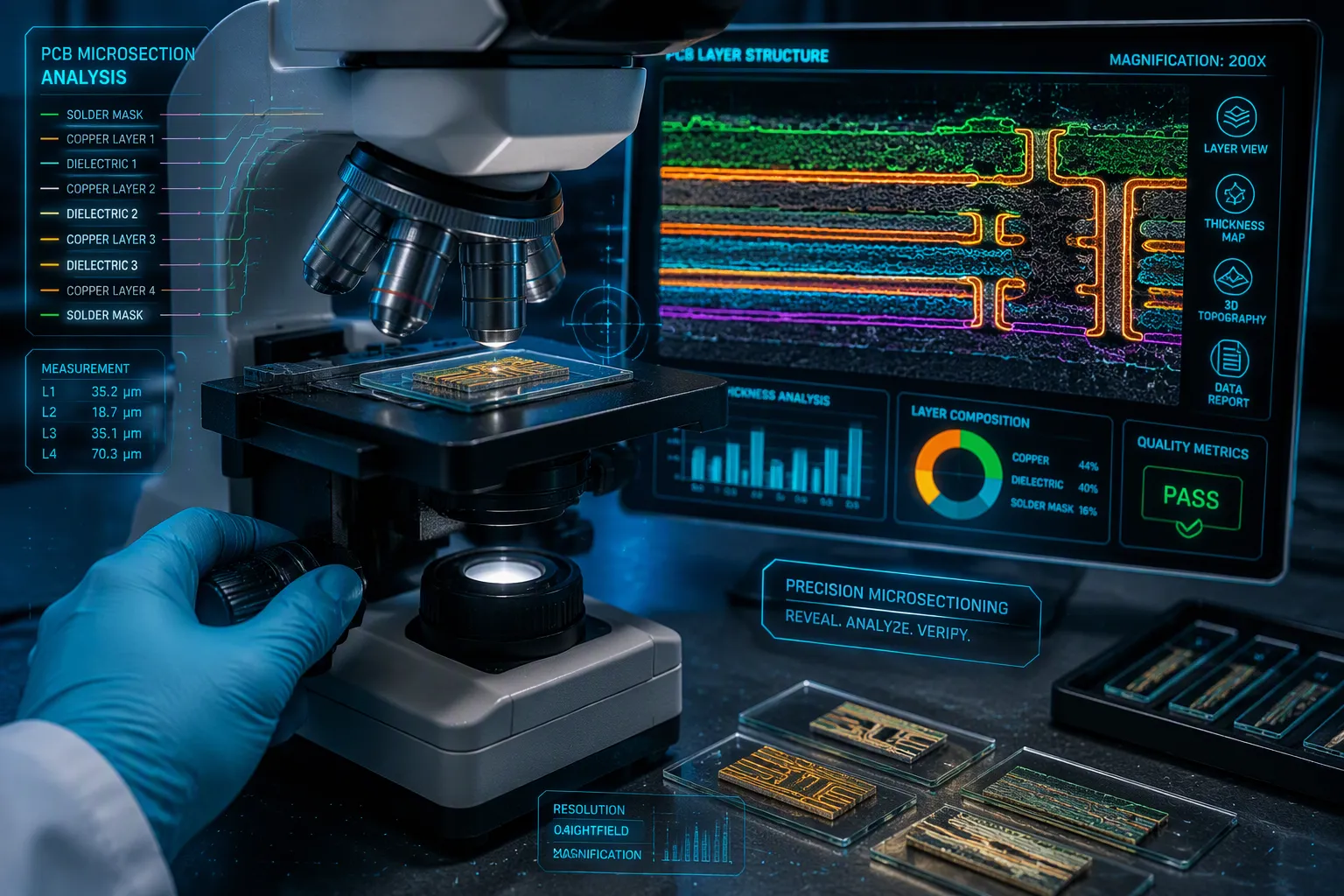
Surface inspection methods compare what you can see. They cannot verify plated barrel integrity or laminate quality. This gap matters when internal defects hide beneath a perfect finish.
Which pcb microsectioning techniques give superior defect detection for your defect types? The answer changes everything.
Microsectioning is a destructive cross-section analysis. It verifies internal plating, via fill, solder joint, and lamination quality. Mechanical microsectioning commonly uncovers incomplete via fills, delamination, and plating problems.
This article compares mechanical microsectioning, precision grinding and polishing, and etching. You will also learn when X-ray, optical inspection, and electrical testing serve as useful complements. Expect a practical selection framework for quality assurance, failure analysis, and high-reliability applications.
Key Takeaways
PCB microsectioning reveals hidden defects that surface inspection cannot see.
Mechanical microsectioning, precision polishing, and etching work together for the best defect detection.
Proper sample preparation prevents artifacts that can mimic real defects.
X-ray and optical inspection are screening tools, not replacements for microsectioning.
Match the microsectioning technique to the defect type and material for superior results.
Follow IPC standards to ensure consistent and reliable microsectioning outcomes.
Use microsectioning for root cause analysis and high-reliability applications.
Why PCB Microsectioning Matters
PCB microsectioning is a destructive cross-section method. It exposes internal PCB structures, plated barrel quality, solder joints, and laminate integrity. You cannot verify these conditions with manual or instrument-based surface inspection methods. Surface methods only compare what they can see. They cannot confirm what happens inside a plated through-hole or between laminate layers.
Mechanical microsectioning helps you identify incomplete via fills, delamination, and plating defects. These problems often stay hidden until field failures occur. A cross-sectional analysis gives you direct visual evidence of internal quality. This evidence supports both process control and failure analysis.
Internal Structures and Plated Features
You use destructive microsectioning to evaluate several critical internal features. The AtlasPCB IPC-TM-650 microsectioning guide lists these commonly verified items:
Copper plating thickness in via barrels and through-holes
Inner-layer registration accuracy
Delamination or voiding
Etch factors
Sequential lamination alignment
Test coupon via types including through-hole, blind, buried, and microvias
The PCBBUY microsection analysis page adds more detail. You can inspect copper plating thickness on outer layers, inner layers, hole walls, and via copper. Hole wall quality and via structures include laser microvias, stacked vias, blind vias, and filled vias. Resin filling quality and via fill integrity also require cross-section analysis of pcbs.
Defects That Demand PCB Cross-Section Analysis
Several defect classes demand PCB cross-section analysis because surface inspection cannot detect them. The BestPCBs cross-section analysis article identifies these commonly checked items:
Plating voids in vias
Insufficient hole wall copper
PCB delamination and microcracking
Etching issues and solder mask overhang
Drilling smear
Uniformity and completeness of copper plating in via holes and through-holes
Laminate, prepreg, and copper foil condition, including voids, resin starvation, and imperfections
Each defect affects reliability differently. Plating voids compromise conductivity. Delamination leads to open circuits or signal loss. Drilling smear prevents proper copper adhesion. You need micro sectioning to see these conditions directly.
How PCB Microsectioning Supports Quality Control
Microsectioning provides a cross-sectional view of the board. Your inspection team can evaluate plating thickness, barrel integrity, internal-layer registration, dielectric condition, and hole quality. These features are not verifiable from the surface. For Class 3 work, tighter acceptance criteria apply to copper plating integrity, hole-wall quality, annular ring, conductor spacing, solder joint acceptability, material control, and process consistency.
The goal is reducing variation, preventing latent defects, and confirming every board meets end-application performance expectations. Vias and plated through-holes in flex and rigid-flex boards must withstand mechanical movement and thermal cycling. Specified inspection methods evaluate plating quality and structural integrity in these high-stress areas.
IPC-A-600 helps evaluate the acceptability and appearance of a finished bare PCB, while IPC-6012 defines the qualification and performance requirements the rigid PCB should meet. They support each other but serve different purposes. For example, an inspector may use IPC-A-600 to evaluate a microsection, while the actual minimum copper thickness or performance requirement may come from IPC-6012 and the customer's drawing. IPC-TM-650 provides a collection of test methods that establish a common testing language so customers, material suppliers, and PCB manufacturers can compare results consistently.
IPC-6012 requires a minimum of 25 microns copper plating thickness for Class 3 high-reliability products. Thin plating risks thermal stress failures. Layer misalignment as small as 50 microns can cause signal integrity issues in high-speed designs at or above 5 GHz. Cracks in solder joints or voids in copper plating are unacceptable. Digital imaging can measure defects like via barrel cracks down to 0.2 microns against IPC-TM-650 criteria. This precision makes microsectioning the verification tool for quality disputes.
How to Compare PCB Microsectioning Techniques
You need a clear framework for evaluating pcb microsectioning techniques. Three main approaches dominate the field: mechanical microsectioning, precision grinding and polishing, and etching. Each method offers distinct advantages for specific defect classes. Your choice depends on the material system, the defect type, and the acceptance criteria you must meet.
A proper technique comparison examines five factors: resolution, measurement accuracy, preparation time, artifact risk, and best-use scenarios. No single method excels at everything. The core lesson is simple. Superior defect detection depends on matching each technique to the material system and defect class.
Mechanical Microsectioning for Plating and Via Analysis
Mechanical microsectioning remains the workhorse for plating thickness and via quality assessment. This destructive, sample-based technique requires you to cut, mount, grind, polish, and etch representative PCB sections. The inspected sample cannot return to production.
The method measures copper thickness at multiple discrete points rather than continuously across the whole board. Localized defects between measurement points may escape detection. Plating uniformity issues such as the hour-glass effect, where the center runs 40–60% thinner than the ends, require careful multi-point measurement to characterize fully.
IPC Class 3 requires that no void exceed 5% of barrel length. This standard means microsectioning must pair with other tests like backlight inspection or IST to fully qualify barrel quality. Thermal stress screening at 288 °C for 10 minutes per IPC-TM-650 is needed after microsectioning to confirm the plating withstands reflow. Cross-sectioning alone does not prove thermal reliability.
Inspection Capability | What Microsectioning Detects |
|---|---|
Copper plating thickness | Outer layer, inner layer, hole wall, and via copper thickness |
Hole wall / barrel quality | Barrel cracks, insufficient copper plating, void formation, resin voids |
Via structures | Laser-drilled microvias, stacked vias, blind vias, filled vias |
Resin filling quality | Improper filling leading to mechanical weakness |
Lamination bonding | Delamination, resin voids, poor press bonding, material separation |
Layer registration | Misregistration, reduced annular ring, via connection problems |
Precision Grinding and Polishing for Accurate Cross-Sections
Precision grinding and polishing determines whether your cross-section reveals true defect geometry or introduces false artifacts. The grinding sequence typically progresses through 400, 600, 800, and 1200 grit silicon carbide paper. Each step runs 30–60 seconds with light pressure.
Best practices minimize damage to delicate PCB layers. Apply minimal pressure to prevent delamination. Use continuous water lubrication to avoid overheating. Rotate the sample 90° between grits to ensure complete scratch removal. Do not over-grind; only remove scratches from the prior step. Inspect frequently under low magnification to monitor progress.
Polishing follows a controlled sequence. Start with 9 μm or 6 μm diamond for initial material removal. Progress to 3 μm, then 1 μm diamond for surface refinement. Finish with 0.05 μm colloidal silica for 1–2 minutes on a soft pad. Always use minimal pressure and keep times short.
Different materials polish at different rates, which can create relief between copper, solder, and substrate. This relief distorts measurements. Controlled removal maintains planarity across phases.
Etching Methods for Microstructural Contrast and Fine Cracks
Etching adds microstructural contrast that mechanical preparation alone cannot achieve. This step reveals grain structure, intermetallic compounds, and fine cracks that polishing may smear over. You apply selective chemical attack to highlight specific phases or defects.
Etching works best as a final step after mechanical microsectioning and polishing. The technique exposes copper grain boundaries and reveals thermal damage patterns. For fine crack detection, etching removes smeared copper that obscures crack tips. Without etching, you might miss hairline fractures that compromise reliability.
The risk of over-etching exists. Excessive chemical attack rounds pore edges and creates false porosity. You must control etch time and concentration carefully. Match the etchant to the material system. Copper responds to different chemistries than solder or laminate.
When you compare pcb microsectioning techniques, remember that etching complements rather than replaces mechanical methods. The best results come from combining mechanical microsectioning and polishing with selective etching. This integrated approach delivers the resolution and contrast needed for superior defect detection.
Defect Detection Capability by Technique
No single pcb microsectioning method catches every defect. Each defect class exposes itself best on a specific cross-section plane and with a specific preparation route. When you match the method to the defect, you improve your effectiveness for defect detection. This section maps the most common internal failures to the technique that reveals them.
Resolution and Accuracy Compared
Resolution describes the smallest feature you can resolve. Accuracy describes how closely your measurement matches true geometry. Mechanical pcb microsectioning delivers strong resolution for plating features, but accuracy depends on sample preparation. Grinding can round edges, polishing can create relief, and etching can widen cracks. Precision grinding and polishing controls those errors. A properly polished cross-section keeps copper, solder, and substrate planar. That planarity lets your measurement system compare features reliably. Digital imaging can measure via wall cracks down to 0.2 microns against IPC-TM-650 criteria. Yet a 0.2 micron measurement means nothing if edge rounding hides the crack tip. Etching improves visibility by removing smeared copper and revealing grain boundaries. Over-etching, however, creates false porosity. The final image quality always depends on the material system and the preparation route.
Plated Through-Hole and Via Defects
Plated through-holes and vias are the most common sites for hidden defects. Stacked microvias over epoxy-filled vias are a particular weak point. Microsectioning verifies fill quality and interface integrity at that junction. For interconnection defect analysis, you need to see both the copper barrel and the interface between fill copper and barrel plating.
Incomplete Via Fills and Plating Voids
The cross-section exposes two different void populations. Voids inside resin or paste arise from trapped air, viscosity, contamination, or via geometry. Plating voids appear inside the copper barrel. Cross-section coupons evaluate fill completeness and residual dimple. Edge voids and center keyhole voids become visible in the plated barrel. IPC-6012 qualification requires at least 32 cross-sections to evaluate void area, dimple, barrel thickness, and fill completeness. That sampling density matters because a single cross-section can miss a localized defect. The method also measures hole wall plating thickness in multiple locations to catch the hour-glass effect. You cannot confirm copper coverage inside a blind via from the surface. Cross-sectioning failed units directly reveals partial voiding and copper coverage below minimum in the barrel. This makes microsectioning the only cited method that directly confirms thickness and coverage inside a via barrel.
Barrel Cracks and Copper Smear
Cracks form at the via knee or along the barrel wall. Copper wall thickness, Z-axis expansion, fill CTE, and thermal cycling all influence their formation. To catch barrel cracks, you must stress the sample first. A 6x solder float at 288°C per IPC-TM-650 2.4.13 is a common thermal-shock qualification. After stress, microsectioned barrel walls are checked for circumferential cracks, delamination, or fill separation. Copper smear, also called pink ring, is a visual signature of incomplete desmear. Resin smear on the barrel wall prevents copper adhesion. Microsection analysis of the barrel wall reveals that smear and the poor adhesion between fill copper and barrel plating. Inadequate desmear is a root cause of edge voids, so the same cross-section can explain both defects.
Solder Joint and Laminate Defects
Via analysis is not the only use. Solder joints and laminate layers also fail beneath the surface. You need different preparation and etching to expose those defects.
Solder Voids and Intermetallic Issues
Solder voids reduce joint strength and create stress concentrators. A cross-section through the joint reveals void size and location. Intermetallic compounds form at the solder-pad interface. Their thickness and morphology control joint reliability. Mechanical polishing alone often smears soft solder over the intermetallic layer. Selective etching removes that smeared solder and exposes the compound. You can then measure the intermetallic layer and judge whether it is brittle. Etch time control remains critical. Over-etching pits the solder and makes voids look larger than they are.
Delamination and Conductive Anodic Filament Defects
Delamination appears as separation between laminate layers or between copper and prepreg. Microsectioning reveals resin voids, poor press bonding, and material separation. Precision grinding with minimal pressure prevents you from manufacturing delamination during preparation. Conductive anodic filament (CAF) grows along the epoxy-glass interface under humidity and voltage bias. CAF testing is a separate reliability test, but cross-sectioning confirms the filament path after failure. Cut the section along the suspected conductor path. Etching can distinguish CAF deposits from normal resin structure.
Early and accurate defect detection depends on choosing the right cross-section plane and the right final etch. Copper plating and plating thickness measurements require a planar polished surface. Verifying copper plating thickness in a stacked microvia demands the same care as checking a through-hole barrel. When you combine mechanical preparation, precision polishing, and selective etching, you can uncover hidden failures before they become field problems.
Sample Preparation for Superior Defect Detection
Microsection/cross-section sample preparation determines whether your results are trustworthy. A perfect technique cannot rescue a poorly prepared sample. The cross-section analysis process begins long before you place the specimen under a microscope.
Microsection and Cross-Section Sample Preparation Steps
Follow a controlled sequence to produce reliable cross-sections. Each step builds on the last one.
Cutting – Select the target area and use a low-speed precision saw with a diamond blade. Keep the sample about 10–15 mm wide and use adequate coolant to produce a clean, flat cross-section without stress or cracks.
Mounting – Fully encapsulate the sample in a cold-mounting epoxy that cures at room temperature. This avoids thermal stress, layer distortion, or delamination.
Grinding – Start with coarse 120-grit silicon carbide paper to flatten the surface. Progress through 400, 800, and 1200 grits using consistent gentle pressure. Clean the sample with isopropyl alcohol or distilled water after each step.
Polishing – Use a polishing cloth with 1 µm or 0.3 µm alumina or diamond slurry to achieve a mirror finish. This makes features like copper plating clearly visible.
Etching – Apply a dilute ferric chloride or ammonium persulfate solution for 10–30 seconds to reveal grain structure or defects. Rinse immediately with distilled water and dry with compressed air to avoid over-etching and residue.
Examination – Inspect the microsection at 50–1000× magnification and record calibrated images for measurement and documentation.
Sample preparation before cross-section also requires you to record sample identity, panel position, cutting orientation, and prior thermal exposure. Keep an unsectioned control sample when comparison may be needed. Define the target plane and remove enough surrounding material to avoid mechanical damage at the feature of interest.
Common Artifacts That Ruin Defect Detection
Preparation artifacts mimic real defects and destroy your credibility. You must recognize them before you report findings.
Edge rounding occurs when grinding pressure is too high or the sample is not properly supported. Copper smear, also called smearing, happens when polishing drags soft copper across the surface. Pull-out removes hard particles and leaves voids that look like plating defects. Epoxy shrinkage creates gaps between the mount and the sample. Excessive etching alters apparent boundaries and creates false porosity.
The following variables directly influence reliability and repeatability, based on IPC-TM-650 2.6.8E referee-procedure guidance:
Sample preparation variable | Influence on reliability/repeatability |
|---|---|
Moisture control / drying | Prescribed drying and desiccator cooling remove uncontrolled moisture; otherwise moisture-driven delamination can be misclassified as a manufacturing defect. |
Coupon representation | The coupon must match the production board's thickness, layer count, material, finish, hole sizes, copper weights, plating process, and connection pattern; a non-representative coupon makes the microsection result unreliable for the actual product. |
Baseline inspection | Pre-exposure inspection and photography document pre-existing blisters, damage, contamination, or suspected delamination, preventing false attribution to the process under evaluation. |
Flux application | Flux type, quantity, coverage, and application method control wetting and thermal contact; excess residue can conceal evidence, so these details must be recorded. |
Bath and surface condition | Verifying solder composition and temperature at the contact surface and removing dross prevents uneven heating and inconsistent thermal load across repetitions. |
Inspection documentation | Recording coupon/hole location, magnification, scale, defect orientation, and acceptance clause ensures that the same defect criteria are applied each time. |
Verification Methods Before Final Inspection
Before declaring a real defect, rule out preparation artifacts such as scratches, edge rounding, copper smearing, pull-out, excessive etch, and off-center sections. This verification step separates skilled analysts from beginners.
Approach the target gradually. Coarse abrasives remove material, while finer abrasives reduce deformation and deep scratches. Polish the exposed face until copper, resin, glass reinforcement, and interfaces are distinguishable. Apply micro-etch only when justified. Excessive etching can alter the apparent boundary and create artifacts.
Precision grinding and polishing controls most artifact risks. Precision grinding and polishing also keeps dissimilar materials planar so measurements remain accurate. When you combine careful preparation with systematic verification, your pcb microsectioning results become defensible. The same discipline applies whether you perform pcb microsectioning for process control or failure analysis. Reliable microsectioning starts with preparation you can repeat. Consistent microsectioning depends on documented procedures and trained analysts. Every microsectioning result reflects the care taken before imaging.
Destructive vs Nondestructive Inspection Methods
You face a clear choice between screening and verification. X-ray, optical inspection, and electrical testing are screening tools. PCB microsectioning is the verification tool. Screening methods flag potential problems across many boards. Verification methods confirm the physical truth on a sample. You need both, but you must never confuse their roles.
The table below summarizes how each method performs against internal defects.
Method | Strength for internal defects | Limitation vs. microsectioning |
|---|---|---|
AOI | Under 10 seconds per standard PCB; ideal for high-volume production. | Checks surface features only; cannot inspect cross-sectional internal structure. |
X-ray (AXI) | Sees through all layers at once for buried vias, blind vias, and BGA joints. | Slower (30 seconds to 1 minute per board) and costlier than AOI; does not replace destructive microsectioning for precise layer-to-layer measurements. |
Electrical testing | Flying probe and fixture tests catch cracks or conductive particles missed by AOI and X-ray. | Verifies electrical paths but cannot measure physical layer thickness, annular ring, or via-barrel integrity. |
Microsection analysis | Provides the clearest internal cross-section: copper thickness, dielectric separation, annular rings, delamination, voids, and via-barrel cracks at 50X–500X. | Destructive, sample-based, and time-consuming; cannot be used on every board. |
X-Ray Strengths and Limits in PCB Cross-Section Analysis
X-ray inspection gives you a non-destructive look inside the board. It reveals hidden structures such as BGA, QFN, and LGA solder joints, voids, hidden bridges, and solder distribution. Modern micro-CT X-ray systems can produce three-dimensional images of internal microstructure at resolutions close to 0.5 micrometers. That resolution helps you locate microcracks. Micro-focus X-ray can also evaluate copper plating thickness uniformity in plated through-hole walls. Keeping wall-thickness uniformity within plus or minus 15 percent under Class 2 is sufficient for consumer electronics conductivity and mechanical strength. Achieving this Class 2 uniformity costs about 30 percent less than meeting Class 3 requirements.
X-ray has hard limits. It cannot show plating thickness with the calibrated precision of a cross-section. It cannot reveal grain structure. Thin delamination and microcracks often escape detection. X-ray does not prove electrical functionality and may not reliably detect every head-on-pillow or non-wet open. CT or cross-sectioning may be required for uncertain cases. When you compare microsectioning vs. x-ray, remember that X-ray shows you where to look. Microsectioning shows you what is actually there.
Optical Inspection and Electrical Testing as Complements
Optical inspection and electrical testing complement your microsectioning work. Pre-reflow AOI checks SMD component presence, orientation, polarity, placement position, and placement conditions. Post-reflow AOI checks visible solder geometry, bridges, tombstones, lifted leads, and other visible workmanship indicators. Reference-based point-to-point comparison and deep-learning inspection extend AOI to surface defects that simple thresholding misses. Electrical testing confirms shorts, opens, resistance, capacitance, and component presence. It can catch physical cracks that visual methods miss.
These methods cannot see beneath opaque packages. They cannot measure physical layer thickness, annular ring, or via-barrel integrity. Microsectioning provides calibrated 1–2 micron measurements that electrical testing cannot deliver. Use AOI and electrical test to localize the fault. Then use pcb cross-section analysis to confirm the root cause.
When to Choose Destructive PCB Microsectioning
Choose destructive microsectioning when you need physical proof. A medical signal-acquisition prototype ran flawlessly under normal lab conditions but dropped its link at random during temperature-cycle reliability testing. The customer revised the layout and re-ordered prototypes, but the fault stayed. Cross-sections prepared by a qualified third-party lab showed micro-cracks in the via barrel copper. Another layout revision would never have found this. The crack sits inside the barrel, and only a cross-section shows it.
On a small-batch IoT controller order, some units behaved unstably. The customer first suspected defective components. The boards were screened with X-ray in-house and samples were sent for metallographic cross-sections. The root cause was excessive voiding inside the BGA solder joints from an unsuitable reflow profile. After the SMT thermal profile was adjusted, the problem was gone. The destructive vs. non-destructive decision comes down to this: screening tells you a fault exists, and pcb microsectioning tells you why. Standardize your preparation procedures, train analysts on artifact recognition, and use microsectioning as the final verification method when quality disputes arise.
Microsectioning Applications in Critical Industries
Quality Assurance and Process Monitoring
You use pcb microsectioning in quality assurance to inspect the internal structure of every production batch. Process monitoring parameters include voids, cracks, laminate voids, delamination, resin recession, inner-layer shorts and opens, trace widths, poor plating, copper thickness, nail heading, lifted pads, registration, and dielectric spacing. Acceptance depends on the absence or acceptable limits of these defects. Level 1 provides quick checks for common failure modes. Level 2 delivers in-depth checks for constructional attributes. Level 3 offers advanced analysis for high-level flaws and thermal stress.
Defect rate targets differ by class. Class 2 production targets less than 1% defects. Class 3 production targets near zero defects. You monitor these targets through statistical process control. This discipline ensures your process stays stable and your product meets customer requirements.
Failure Analysis and Root Cause Identification
When a board fails in the field, you need to know why. Microsectioning per IPC-TM-650 2.1.1 examines base material, plated through holes, internal copper conductors, and internal ground, power, and thermal planes. Cross-section observations identify laminate defects such as delamination, blistering, cracks, ground-plane clearance, and layer-to-layer spacing. Plated through-hole defects include hole-size problems, annular-ring problems, nailheading, plating-thickness defects, plating voids, nodules, cracks, resin smear, etchback issues, wicking, inner-layer separation, and solder mask thickness. Internal conductor defects include over-etch, under-etch, conductor cracks, voids, uneven oxide treatment, and foil thickness.
These observations support failure analysis directly. Plated through-hole cracks, voids, and resin smear root-cause PTH failures. Laminate delamination, blistering, and cracks root-cause laminate failures. Conductor cracks, voids, or poor plating can cause or reveal weakened solder joints. You trace each failure to its physical origin.
High-Reliability Standards for Space, Defense, and Medical Electronics
High-reliability sectors demand components that meet strict performance criteria under harsh conditions. Flight control systems in aerospace, life-support equipment in medical devices, and communication systems in military operations face temperature extremes, vibration, and radiation exposure. IPC Class 3 applies to aerospace, defense, and critical medical machinery where failure may cause severe damage. Quality control includes 10x magnification inspection, automated optical inspection, stringent plating thickness requirements of minimum 25 microns for through-holes, 75% barrel fill for PTHs, and comprehensive documentation with complete traceability.
IPC-A-600L guides incoming inspection protocols to identify issues before components enter systems. JEDEC J-STD-020E provides guidelines for evaluating moisture and reflow sensitivity, which matters in humid or variable climates. Automotive electronics, 5G infrastructure, and telecom equipment also rely on microsectioning for process validation. Regulatory compliance from IPC standards, ISO quality systems, and product-safety regulations pushes OEMs and EMS providers to adopt rigorous microsection testing. You add microsectioning to multi-stage inspection processes to verify internal structures like plating quality.
Choosing the Right Technique for Superior Defect Detection
Decision Factors: Defect Type, Material, and Goal
Your first decision factor is the defect type. Copper thickness, via integrity, delamination, and contamination each demand a different preparation route. Mechanical microsectioning exposes buried defects such as incomplete via fills, cracks, and delamination. Etching reveals grain boundaries, open circuits, shorts, and extra copper. Match the technique to the defect you need to find.
Material properties shape your second decision. PCB complexity and layer count matter. Simple boards may require only basic sectioning. Multilayer or fine-feature boards need precision polishing and possibly SEM-level inspection. Consider material variability and heat sensitivity as well.
Material-specific challenges should guide preparation: PCBs are made of composite materials such as FR-4 with differing hardness, making uniform grinding difficult, and excessive heat can melt solder or epoxy. Thus, equipment with cooling and controlled material removal is essential. Etching is an optional, post-polishing chemical step used to enhance features such as copper grain boundaries and otherwise invisible defects; its parameters must be controlled so it does not hide or alter the true defect structure.
Your analytical goal forms the third factor. Do you need SEM/EDS or advanced analysis? Precision grinding and polishing must produce a smooth, artifact-free cross-section to support high-magnification imaging and elemental analysis. Sample volume, cost, and destructiveness also guide your choice. Microsectioning destroys the sample. Use test coupons for expensive boards and faster methods for high-volume testing.
Cost, Time, and Skill Trade-Offs
Budget constraints affect your technique selection. Mechanical microsectioning costs less than precision grinding and polishing with SEM follow-up. Etching adds minimal cost as a post-polishing step. High-volume testing favors faster methods. Expensive boards justify test coupons to avoid destroying production units.
Time requirements vary by technique. Basic mechanical sectioning takes less time than precision polishing. Etching adds only minutes to your process. Skill level matters most for artifact recognition. Standardized grinding and polishing procedures reduce training time. Controlled etching demands experience to avoid over-etching. Your team's expertise determines which pcb microsectioning techniques you can execute reliably.
A Simple Selection Framework for PCB Microsectioning
Follow this four-step framework for choosing the right technique. First, identify the defect. Second, match the technique to the material system and defect class. Third, verify sample quality before imaging. Fourth, evaluate results against acceptance criteria.
Category | Selection Factor | Implication for Technique Choice |
|---|---|---|
Defect-specific | Target defects: copper thickness, via integrity, delamination, contamination | Mechanical microsectioning exposes buried defects; etching reveals grain boundaries and shorts |
Material-specific | PCB complexity and layer count | Simple boards need basic sectioning; multilayer boards need precision polishing |
Material-specific | Material variability and heat sensitivity | Choose controlled grinding with coolant to prevent artifacts |
Analytical goal | Need for SEM/EDS or advanced analysis | Precision polishing must produce artifact-free cross-sections |
Analytical goal | Sample volume, cost, and destructiveness | Use test coupons for expensive boards |
Analytical goal | Preparation quality and application fit | Standardized procedures reveal only real defects |
Standardized grinding and polishing and controlled etching avoid scratches and smearing. This approach reveals only real defects and matches the method to design rules and reliability goals. Your pcb microsectioning delivers superior defect detection when you follow this disciplined framework.
No single method wins every case. Superior defect detection combines mechanical cross-sectioning, precision polishing, and selective etching. Each technique exposes different flaws.
Sample preparation remains the real differentiator. Grinding and polishing artifacts like smearing, edge rounding, or copper pull-out ruin even the best technique. You must control every step.
X-ray, optical inspection, and electrical testing serve as screening tools. They cannot substitute for pcb microsectioning. Use them to localize faults, then confirm with destructive microsectioning.
Build a decision matrix from defect type, material system, and acceptance criteria. IPC standards provide your baseline. Standardize preparation procedures, train analysts on artifact recognition, and apply microsectioning as final verification whenever quality disputes arise.
FAQ
What is PCB microsectioning?
PCB microsectioning is a destructive cross-section method. It exposes internal structures like plated barrels, solder joints, and laminate layers. You cut, mount, grind, polish, and etch a sample. This process reveals defects that surface inspection cannot detect, including plating voids, delamination, and incomplete via fills.
Which microsectioning technique gives the best defect detection?
No single technique wins every case. Mechanical microsectioning exposes buried defects like cracks and incomplete fills. Precision polishing keeps materials planar for accurate measurement. Etching reveals grain boundaries and fine cracks. You achieve superior detection by combining all three methods and matching them to your defect type.
Can X-ray replace PCB microsectioning?
No. X-ray is a screening tool. It shows you where to look but cannot measure plating thickness with calibrated precision. X-ray cannot reveal grain structure, thin delamination, or microcracks. Microsectioning provides the physical proof that X-ray cannot deliver. Use X-ray to localize faults, then confirm with cross-section analysis.
What defects require PCB cross-section analysis?
Several defect classes demand cross-section analysis. These include plating voids in vias, insufficient hole wall copper, delamination, microcracking, drilling smear, and incomplete via fills. You also need microsectioning to verify copper plating thickness, inner-layer registration, and resin filling quality. Surface methods cannot detect these internal conditions.
How do you prepare a PCB microsection sample?
Follow a controlled sequence. Cut the target area with a low-speed precision saw. Mount the sample in cold epoxy. Grind through 400, 600, 800, and 1200 grit papers. Polish with diamond slurry down to 0.05 μm colloidal silica. Etch for 10–30 seconds to reveal microstructure. Inspect at 50–1000× magnification.
What artifacts ruin microsection defect detection?
Common artifacts include edge rounding, copper smear, pull-out, and epoxy shrinkage. Over-etching creates false porosity. These artifacts mimic real defects and destroy your credibility. You must recognize them before reporting findings. Precision grinding with minimal pressure and controlled etching times prevent most artifact risks.
When should you choose destructive microsectioning?
Choose destructive microsectioning when you need physical proof. Screening methods tell you a fault exists. Microsectioning tells you why. Use it for root cause analysis, quality disputes, and high-reliability applications. It verifies plating thickness, barrel integrity, and laminate quality against IPC-6012 and IPC-A-600 acceptance criteria.
What standards govern PCB microsectioning?
IPC-6012 defines qualification and performance requirements for rigid PCBs. IPC-A-600 guides acceptability evaluation of finished boards. IPC-TM-650 provides test methods for thermal stress and microsectioning procedures. These standards establish a common testing language. They ensure consistent results across customers, material suppliers, and manufacturers.
