A Complete Guide to Multilayer PCB Manufacturing in 2025
Multilayer PCB manufacturing in 2025 is driving innovation in electronics. The multilayer PCB manufacturing industry is expanding rapidly, with the global market size projected to reach between $81 and $92 billion:
Source | Year | Market Size (USD Billion) |
|---|---|---|
SkyQuest | 2023 | 81–92 |
The multilayer PCB manufacturing process involves advanced stackup design, precise via formation, and rigorous quality control.
Key advancements in multilayer PCB manufacturing include miniaturization, HDI, flexible substrates, and embedded components. These improvements enhance stackup design and overall PCB performance.
Key Takeaways
Multilayer PCBs have many copper layers with insulation between them. This lets more circuits fit in a small space. It helps devices work better and be smaller. Devices like smartphones, cars, and medical machines use these boards.
Picking the right materials is important. You must also design the stackup and vias carefully. This gives strong signals and less interference. It makes the boards last longer and fit your device’s needs.
You need to follow exact steps to make these boards. Using automation and AI inspection helps a lot. Working with good suppliers is important too. These things help make multilayer PCBs with fewer mistakes and better quality.
Multilayer PCBs
Structure
A 4-layer pcb looks more complicated than single- or double-layer boards. It has at least three copper layers, with insulation between each one. In a 4-layer pcb, there are two signal layers and two inner layers. The inner layers are usually for power and ground. This design lets you fit more circuits in a small area. You can use different vias, like through-hole, blind, and buried vias. These vias help connect the layers and move signals between them. The inner layers often work as power or ground planes. This helps stop electromagnetic interference and makes signals clearer. You can see the differences in the table below:
PCB Type | Construction Characteristics | Routing Capabilities | Applications and Advantages | Limitations and Complexity |
|---|---|---|---|---|
Single-Layer | One copper layer on one side of substrate; components on opposite side | All traces on one plane; no crossover without jumpers | Simple devices; low cost; easy to produce and repair | Limited routing; low component density; no EMI shielding; larger board size due to routing constraints |
Double-Layer | Copper on both sides; vias connect layers; components on both sides | Two planes for routing; can cross traces using both sides | Medium complexity circuits; better space use; moderate cost; higher component density than single-layer | More complex manufacturing; limited for high-speed or very complex circuits; limited EMI shielding |
Three or more copper layers separated by insulation; inner layers often power/ground planes | Complex routing; dedicated power/ground planes; controlled impedance; signal isolation | High-density, complex, high-speed, RF applications; highest component density; superior electrical performance; better EMI shielding; smaller size | Higher manufacturing cost; longer production; complex design; harder to test and repair |
Applications
You can find 4-layer pcb designs in many modern products.
4-layer pcb boards are used in smartphones and laptops.
Car makers use 4-layer pcb technology for electric vehicles and ADAS.
Airplanes use 4-layer pcb modules for flight control and navigation.
Factories use 4-layer pcb boards for strong signals and long life.
Medical machines, like imaging tools, need 4-layer pcb reliability.
Telecom equipment uses 4-layer pcb designs for fast logic and RF circuits.
The military uses 4-layer pcb boards for important missions.
Tip: Pick a 4-layer pcb if you need lots of parts, strong signals, and good performance in tough places.
Materials
Substrates
When you pick materials for a 4-layer pcb, you must think about how it will work. The right substrate makes your multilayer pcb strong, bendable, and dependable. Here are the main substrates used in multilayer pcb manufacturing:
FR-4: This is a fiberglass and epoxy resin. It is the most common choice for 4-layer pcb designs. It gives good strength, keeps electricity safe, and does not cost too much.
Polyimide: You use this flexible material in flex and rigid-flex multilayer pcb boards. It can handle heat and chemicals well.
Rogers: This is a polymer-ceramic mix. It works best in high-frequency multilayer pcb jobs. It keeps signals clear and steady.
Metal-core substrates (like aluminum): These help control heat in high-power 4-layer pcb circuits.
Ceramic-based substrates (such as alumina): You find these in special multilayer pcb designs that need to stay cool.
Tip: Picking the right material for multilayer pcbs helps you get the best mix of price, performance, and dependability.
Copper Layers
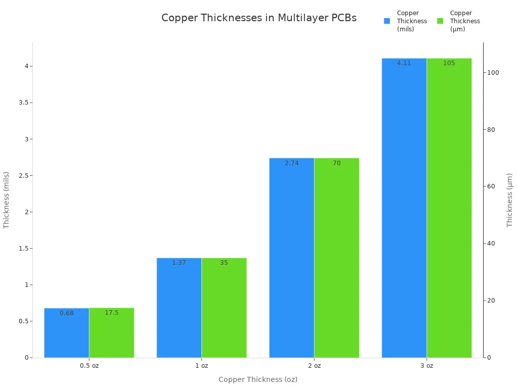
Copper layers move signals and power in your 4-layer pcb. You must choose the right thickness for each layer in your multilayer pcb. Thin copper is good for inside layers. Thick copper is better for outside layers that carry more current. The table below shows common copper thicknesses used in multilayer pcb manufacturing:
Copper Thickness (oz) | Thickness (mils) | Thickness (µm) | Typical Use Case | Minimum Pattern Width/Spacing (mils) |
|---|---|---|---|---|
0.5 | 0.68 | 17.5 | Inner layers, low power applications | ~3.5 / 3.5 |
1 | 1.37 | 35 | Standard PCB layers (outer layers) | ~4 / 4 |
2 | 2.74 | 70 | High current, heavy copper PCBs | ~6-10 / 8-10 |
3 | 4.11 | 105 | Heavy copper for high current density | ~7-15 / 12-15 |
Innovations
New materials and methods are changing how you make a 4-layer pcb. Many multilayer pcb makers now use high-frequency dielectrics like Rogers for signal layers. They mix these with cheaper FR-4 for power and ground layers. This mix helps signals stay strong and saves money. Some companies use new via methods, like laser drilling, to make better connections. New resin systems and special low-loss materials can make high-frequency multilayer pcb boards up to 30% cheaper. Surface finishes like ENIG also make boards last longer, even if they cost more than old finishes.
Multilayer PCB Manufacturing Process
Design
You begin making a multilayer pcb by planning carefully. Good design helps you avoid mistakes later. Here are the main steps you should follow:
Decide what you want your pcb to do and where it will be used.
Draw a clear schematic. This shows all the parts and how they connect.
Place each part in a smart spot. Think about how heat moves and how signals travel.
Draw the paths for signals. Keep them short and direct. Use tools to check your work.
Test your design. Look for mistakes before making the board.
Keep all your design files and instructions neat and easy to find. This helps you make better boards and saves time.
Inner Layer Etching
Inner layer etching shapes copper on the inside layers. You use photoresist to protect copper you want to keep. Then, you spray chemicals to remove extra copper. Ferric chloride and cupric chloride are common chemicals. Ammonium persulfate is used for very careful jobs, but it works slower.
Method | Chemicals Used | Application | Notes |
|---|---|---|---|
Acid Etching | Ferric chloride, Cupric chloride | Inner layer etching | Precise, small undercuts, best for inner layers |
Alkaline Etching | Amination | Not used for inner layers | |
Photoresist Use | Photoresist as etch resist | Inner layers | Protects copper during etching |
You must watch the speed, strength, and time of etching. This step is important for the rest of the process.
Stack-Up
Stackup design is the base of every multilayer pcb. You put copper and insulation in a set order. A good stackup keeps signals clear and the board flat. Put signal layers next to power or ground planes. This helps signals and stops noise.
Put ground vias close to signal vias for better paths.
Do not leave gaps under signal and power lines.
Use even stackups to stop bending.
Use tools to check your stackup before building. A good stackup keeps signals strong and heat under control.
Lamination
Lamination sticks all the layers of your pcb together. You stack prepreg and copper foil in the right order. Then, you press them with heat and pressure. The prepreg melts and glues the layers, pushing out air.
Lamination makes strong bonds between layers.
It stops layers from coming apart.
This step is important for strong and long-lasting boards.
Drilling & Vias
Drilling makes holes for vias that link layers. You use both machines and lasers. Lasers make tiny microvias for tight designs.
Lasers do not wear out and are very exact.
Machines drill bigger holes and work fast.
You can make blind, buried, and stacked vias for tricky paths.
Place vias in smart spots to keep signals and power strong.
Plating
Plating covers holes and copper with a thin metal layer. This step makes sure layers connect with electricity. You must watch thickness, stickiness, and evenness.
Clean the board well before plating.
Watch heat, current, and time closely.
Use copper, gold, nickel, or tin as needed.
Even plating keeps signals strong and the board working well. Check thickness and stickiness to make sure it is right.
Outer Layer Etching
Outer layer etching makes the final copper shapes. This step is harder than inner layer etching. You add photoresist, plate with tin, then remove extra copper. The tin keeps the copper you want.
Outer layers need tighter lines and careful etching.
After etching, take off the tin and check for extra copper.
AOI checks the patterns for mistakes.
Outer layer etching needs care to stop problems, especially for fast boards.
Solder Mask
The solder mask protects your pcb from shorts and rust. It covers everything except the pads for parts. The most used solder mask is LPI. LPI gives sharp lines for small parts.
Epoxy masks are tough and fight chemicals.
Dry film masks are even and good for strong boards.
New ways like LDI and inkjet printing give more detail.
Watch the thickness and space of your solder mask. This stops solder bridges and helps place parts right.
Surface Finish
Surface finish covers copper pads to stop rust and help soldering. You can pick from many finishes:
HASL is cheap but not flat enough for tiny parts.
ENIG is flat, fights rust, and is good for tight boards.
Immersion silver and tin are good for soldering but can tarnish.
OSP is safe for the earth but does not last long.
Surface Finish | Description | Impact on Performance |
|---|---|---|
HASL | Tin-lead solder, uneven surface | Tough, cheap, not for tiny parts |
ENIG | Nickel and gold layers | Flat, rust-proof, reliable |
Immersion Silver | Silver coating | Good for soldering, can tarnish |
OSP | Organic coating | Eco-friendly, short life |
Pick the finish that fits your board, where it will be used, and your budget.
Silkscreen
Silkscreen printing puts labels and numbers on your pcb. This helps you find parts when building or fixing. Follow these tips for good silkscreen:
Use clear letters and put them in the right place.
Leave at least 0.005 inches between silkscreen and pads.
Do not print over pads or vias.
Use easy-to-read fonts and sizes.
Pick the best printing way: by hand, photo, or direct print.
Line up text for easy reading and use bright colors.
Good silkscreen makes your board easier to build and check.
Testing
Testing checks your pcb for problems before shipping. You use different ways:
AOI finds missing parts or solder bridges.
X-ray looks inside for hidden problems.
Functional testing checks if the board works right.
Boundary scan helps with tight boards you cannot reach.
No one test finds every problem. Use a mix of tests to catch all mistakes and make sure your board is good.
Profiling
Profiling cuts finished boards from the panel. You can use different ways:
V-cut scoring makes grooves for easy breaking. It gives clean edges and less stress.
Router cutting uses a spinning tool for smooth and tricky shapes.
Laser cutting is very exact and good for tight shapes.
Punching is fast for lots of boards but may leave rough edges.
Profiling Technique | Working Principle | Advantages | Limitations | Applications |
|---|---|---|---|---|
V-Cut Scoring | V-grooves for breaking | Clean edges, low stress | Only simple shapes | Mass production, rigid/flex boards |
Router Cutting | Rotating tool cuts shape | Smooth edges, flexible | Debris, tool wear | Prototyping, small batches |
Laser Cutting | Laser vaporizes material | Very exact | Costly, slower | High-end, flex boards |
Punching | Mechanical punch | Fast, automatic | Rough edges | High-volume |
Pick the profiling way that fits your board design, how many you need, and the quality you want.
Technologies & Trends
Automation
Modern multilayer pcb factories use a lot of automation. These new tools help make pcbs faster and with fewer errors. Some of the latest automation tools are:
Artificial Intelligence helps plan work and tells you when machines need fixing.
IoT devices watch machines all the time and help you use data to make smart choices.
Advanced robotics, like cobots, pick up small parts and put them together very carefully.
Digital Twin technology lets you test your assembly line on a computer before you build it.
Eco-friendly machines and materials save energy and help the earth.
Flexible automation systems let you make different multilayer pcb boards when you need them.
Description and Benefits | |
|---|---|
Automated machinery | Drills, solders, and puts parts on fast and right. |
Automated Optical Inspection | Finds mistakes quickly and helps make better boards. |
Advanced Robotics (Cobots) | Puts parts in place and does hard jobs well. |
Digital Twin Technology | Tests steps on a computer to plan better and make fewer mistakes. |
AI Inspection
Artificial intelligence can check multilayer pcb boards for problems. Deep learning models, like convolutional neural networks, look at pictures from many sides to find mistakes. These AI systems can see broken lines, missing parts, or bad solder spots. They learn from your feedback and get smarter over time. AI checks boards faster and better than people. It also makes fewer mistakes and keeps quality high. You can trust AI to find even tiny problems, which helps your boards work better and cost less.
HDI
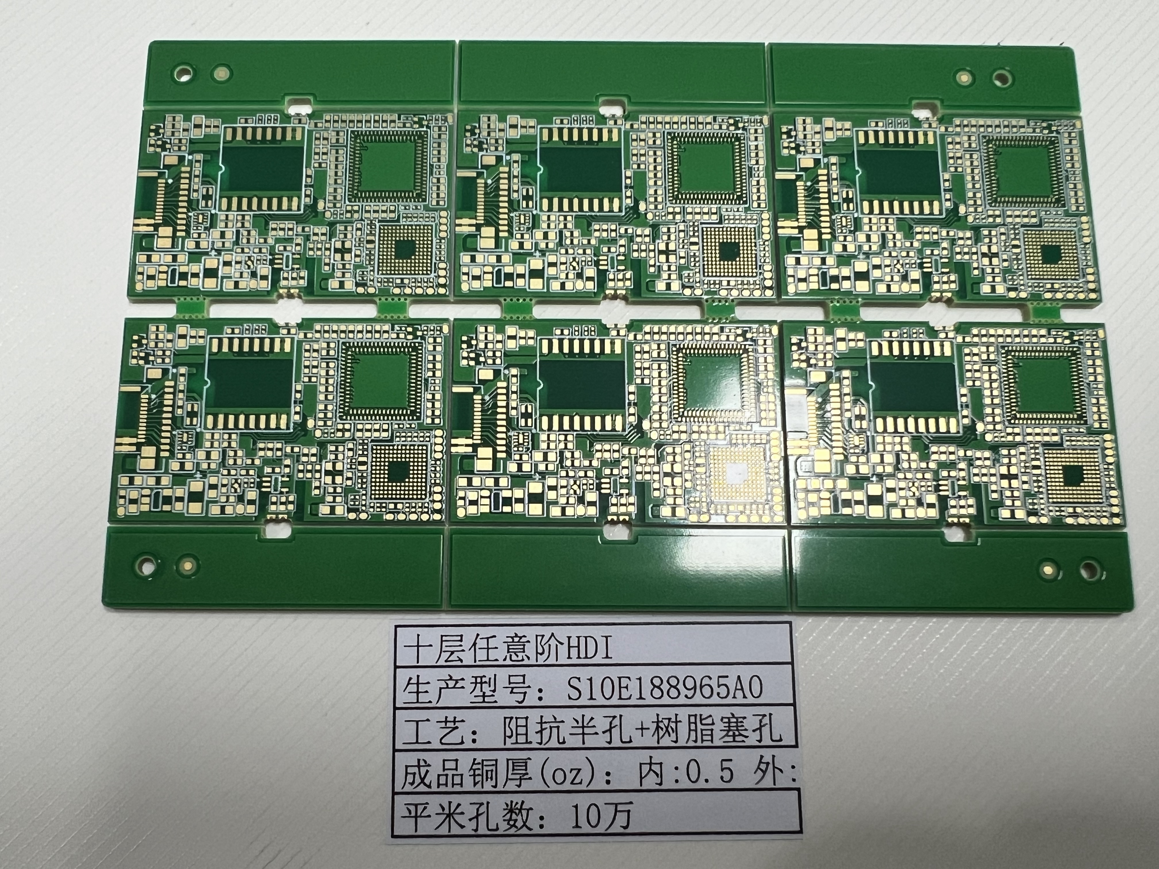
High-density interconnect, or HDI, lets you put more circuits in a small multilayer pcb. You use special vias, like microvias, blind vias, and buried vias, to connect layers. Microvias are very small and made with lasers, so you can fit wires in tight spaces. HDI pcb boards use a step-by-step process to stack layers and make tricky connections. You get thinner lines, smaller holes, and more pads in one spot. HDI gives you smaller boards, better signals, and strong multilayer pcb designs for new electronics.
HDI types are 1+N+1, 2+N+2, and any-layer HDI, with more microvia layers for higher density.
You see HDI in smartphones, tablets, and other small devices.
Green Manufacturing
You can help the earth by picking green manufacturing for your multilayer pcb projects. Many factories now use safe materials, like lead-free solder and halogen-free boards. They recycle copper and chemicals to make less trash. Machines that use less energy, like LED curing systems, save power. Some factories use solar or wind energy to make less pollution. You can design your pcb to be easy to recycle by using less copper and making smaller boards. Following rules like RoHS and ISO 14001 also keeps your work safe for the planet.
Challenges & Solutions
Registration
You must line up each layer very carefully in a multilayer pcb. If layers do not match, you might get shorts or broken paths. Drill registration is hard because every layer can need different hole sizes. Sometimes, pipes get stuck or holes get dirty during making. You can fix these by using good drilling machines and keeping them clean. X-ray machines help check if holes are in the right place. Automated alignment systems can spot mistakes early. Pick a manufacturer who knows how to make multilayer pcb boards well.
Challenge | Solution |
|---|---|
Drill Registration | Use precise drilling equipment, regular calibration, and X-ray inspection |
Layer Misregistration | Use stable materials and automated alignment systems |
Warping
Warping means your multilayer pcb bends or twists. This happens when copper and the board grow at different speeds or copper is not even on each layer. You can stop warping by making a balanced stack-up and picking materials that act the same with heat. Keep your pcb in a dry, cool place to stop water from causing trouble. Baking the pcb after pressing helps let out stress. Always use fabricators who know how to stop warping in multilayer pcb boards.
Make copper layouts even.
Use stack-ups that are the same on both sides.
Pick materials that grow the same with heat.
Watch the heat during making.
Store boards in dry, cool places.
Signal Integrity
Signal integrity means signals stay clear and strong in fast multilayer pcb designs. You can keep signals good by putting solid ground planes under signal layers. Keep traces short and far apart to stop crosstalk. Use differential pairs for fast signals and do not run sensitive lines next to each other. Pick materials that keep electricity steady. Put decoupling capacitors close to power pins to cut noise. Work with your manufacturer to make sure your pcb design keeps signals strong.
Use ground planes that do not break.
Route differential pairs close together.
Keep fast traces away from each other.
Control impedance with the right trace width and space.
Yield
Yield tells you how many good pcb boards you get from a batch. Many things can make yield lower in multilayer pcb making. More layers, smaller holes, and tight spaces make it harder. Hard designs and thick copper can cause more mistakes. You can get better yield by following rules for easy making and using normal parts. Pick the best materials and finishes for your pcb. Work with skilled makers to cut mistakes and get more working multilayer pcb boards.
Factor | Impact on Yield |
|---|---|
More layers lower yield | |
Trace Width/Spacing | Smaller sizes increase defects |
Drill Hole Size/Count | More or smaller holes lower yield |
Material Choice | Stable materials improve yield |
Good design raises yield |
PCB Quality Control
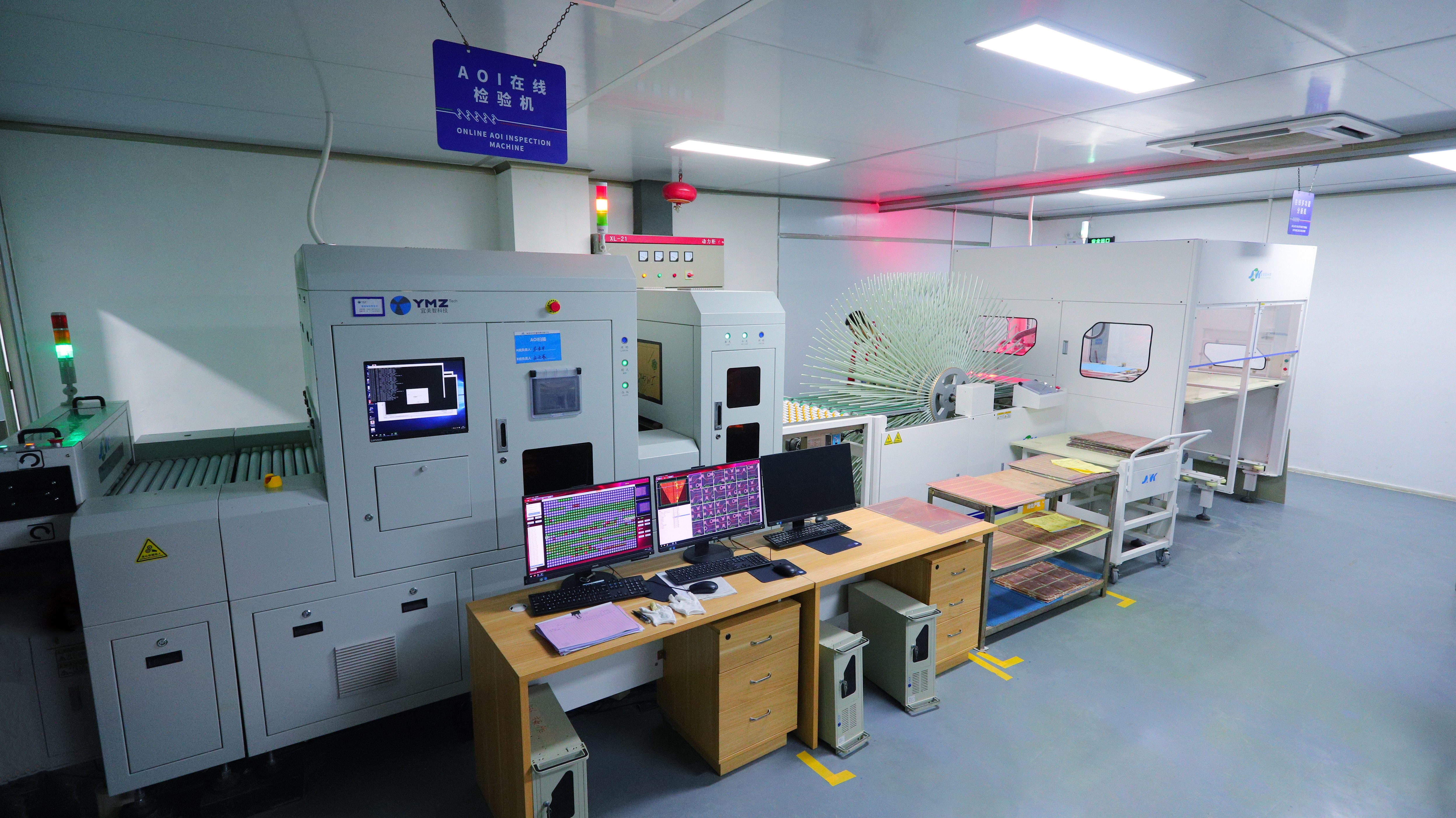
AOI
Automated Optical Inspection, or AOI, helps find problems fast. AOI uses cameras and lights to look for issues on your pcb. It checks for things like scratches, stains, or missing parts. You do not have to touch the board during this check. The system takes pictures from many angles. It uses smart software to spot even small mistakes. AOI works quickly and fits into modern pcb factories. You can count on AOI to find open circuits, solder bridges, or wrong parts. Many AOI machines use robotic arms and sharp cameras to scan every area. This way, you get good results and keep your boards high quality.
AOI uses LED lights from different sides to stop shadows.
Sharp cameras can take up to 100 pictures each second.
The software finds problems using pattern matching and machine learning.
AOI machines often read barcodes to track each board.
AOI is very important for checking complex multilayer pcb boards.
X-ray
X-ray inspection lets you see inside your pcb without breaking it. This method uses X-ray beams to make 2D and 3D pictures of the inside layers. You can find hidden problems like solder gaps, blocked vias, or cracks you cannot see. X-ray checks are needed for boards with many layers or parts like BGAs. High-quality X-ray machines can spot tiny cracks or parts that are not lined up. You get instant feedback, so you can fix problems early and save money. X-ray checks help your pcb stay safe and work well in important devices.
X-ray finds hidden problems like gaps, cracks, and parts in the wrong place.
3D X-ray and CT scans show slices of your pcb.
This process does not hurt the board and is safe.
Electrical Tests
Electrical tests make sure your pcb works the right way. You can pick different tests for your needs. In-Circuit Testing, or ICT, checks each part for shorts, opens, and solder issues. This test is quick and good for big batches. Flying Probe Testing uses moving probes to check for mistakes and does not need special tools. This is good for new designs or small numbers. Burn-in testing runs your pcb hot and busy to find weak spots early. You can also use continuity, resistance, and functional tests to check if everything connects and works. The table below shows common electrical test types:
Test Method | Purpose / Focus | Advantages / Notes |
|---|---|---|
In-Circuit Testing | Checks each component for defects | Fast, accurate, best for high-volume production |
Flying Probe Testing | Uses moving probes for flexible testing | Good for prototypes and small batches |
Burn-In Testing | Runs board under stress to find early failures | Ensures long-term reliability, used for critical uses |
Continuity Testing | Verifies all connections | Prevents open circuits and broken wiring |
Functional Testing | Tests board in real-world conditions | Confirms design works as expected |
Picking the right electrical test helps you deliver a reliable pcb every time.
Best Practices
DFM
Design for manufacturability, or DFM, means making your pcb easy to build and test. You should start thinking about DFM at the beginning of your project. Use normal part sizes and make sure labels are easy to read. Keep trace widths and spaces within what your manufacturer can do. Put test points where they are easy to reach. If you follow DFM rules, you save time and money. Your pcb will work better and have fewer problems.
Tip: Ask your manufacturer for their DFM checklist before you finish your design.
Supplier Choice
Choosing the right supplier is very important for your pcb. Find suppliers who have done good work before. Make sure they have the right certifications. Ask them about how they check quality. If you can, visit their factory to see how they work. Good suppliers answer your questions fast and help fix problems. They also give clear prices and deliver on time.
What to Check | Why It Matters |
|---|---|
Certifications | Shows quality and safety |
Lead Times | Helps you plan better |
Support | Solves issues quickly |
Documentation
Clear documentation helps everyone know what to do in your pcb project. You should add drawings, lists of parts, and notes for building. Good documentation makes it easier to fix mistakes and build the board right. Use simple words and clear pictures. Keep your files neat and up to date. When you share good documentation, your team and supplier can work faster and make fewer mistakes.
Note: Good documentation can stop delays and help save money.
You can get really good at making multilayer PCB boards if you follow every step carefully. Pay attention to how you stack the layers and where you put the vias. Always check your work to make sure it is right.
Write down your steps so others can follow them.
Pick suppliers you know you can trust.
Always be ready to learn about new tools and ideas. This will help you make stronger and better boards.
FAQ
What is the main benefit of using multilayer PCBs?
You can fit more circuits in a smaller space. This helps you build faster, smaller, and more reliable electronic devices.
How do you choose the right PCB material?
You should look at your device’s needs. Pick materials that match your heat, strength, and signal requirements.
Why are vias important in multilayer PCB design?
Vias connect different layers. You use them to move signals and power between layers. Good via placement improves board performance.