Cost-Benefit Analysis of Advanced HDI PCB Technologies: Stacked and Staggered Microvia Structures for Next-Generation Electronics
Cost-Benefit Analysis of stacked and staggered microvias in HDI PCB manufacturing reveals important trade-offs for next-generation electronics. Microvias play a key role in HDI PCBs, supporting the miniaturization and complexity required by modern devices. LT CIRCUIT delivers solutions that address these challenges with advanced PCB technology and reliable processes.
The 'HDI Microvia PCB Market Report: Trends, Forecast and Competitive Analysis to 2031' by Lucintel notes rapid advancements in microvia technology, including laser drilling and automated manufacturing. Manufacturers use high-frequency laminates and eco-friendly substrates to improve PCB performance and sustainability.
Microvias enable higher-density interconnects in HDI PCBs, which power telecommunications, automotive, and medical devices. LT CIRCUIT’s expertise ensures each PCB meets strict industry standards for reliability and value. Decision-makers should weigh performance, reliability, and overall value when selecting microvia structures for HDI PCBs.
Key Takeaways
Stacked microvias save space and boost circuit density, making them ideal for compact, high-speed electronics, while staggered microvias offer better reliability and simpler manufacturing for multi-layer PCBs.
Advanced laser drilling reduces manufacturing costs and enables smaller, more precise microvias, supporting high performance and efficient production in next-generation devices.
LT CIRCUIT combines expert design, strict quality control, and advanced manufacturing to deliver reliable, high-quality HDI PCBs tailored to diverse industry needs.
Microvias in HDI PCBs
Stacked Microvias Overview
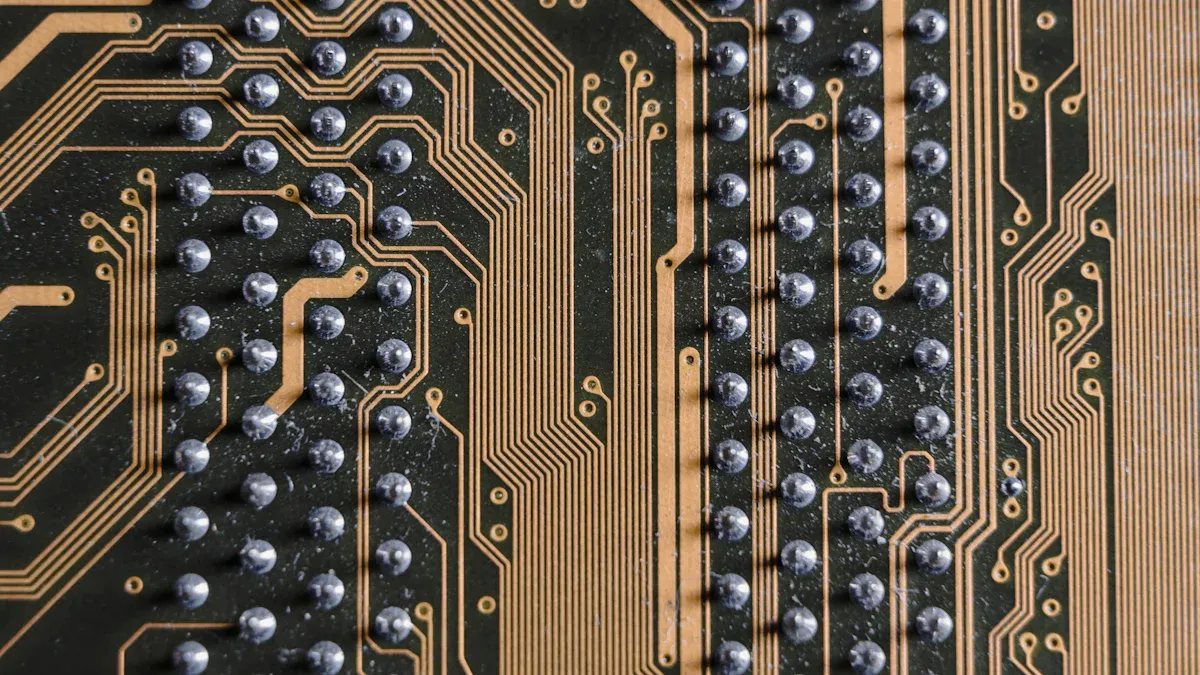
Stacked microvias play a key role in HDI PCB technology. Engineers use stacked microvias to create vertical connections through multiple layers. This approach saves space and increases circuit density. Stacked microvias align directly above each other, forming a straight path for electrical connections. This structure supports high density interconnects and advanced via structures. Designers often choose stacked microvias for compact devices that demand reduced board space and high-density interconnect. The process requires precise alignment and copper filling to ensure strong connections between layers. Stacked microvias offer excellent signal integrity and consistent impedance, making them ideal for high-speed circuits.
Staggered Microvias Overview
Staggered microvias use an offset pattern for connections between layers. Each microvia sits beside, not above, the one on the next layer. This design spreads connections across the PCB, reducing stress on any single point. Staggered microvias improve reliability, especially in PCBs with many layers. The manufacturing process is less complex because copper filling is often not required. Staggered microvias handle thermal and mechanical stress better, making them suitable for multi-layer HDI designs. They support advanced via structures and help maintain strong connections in high-density environments.
Key Differences
The choice between stacked microvias and staggered microvias affects space, density, and reliability. Stacked microvias save space by aligning connections vertically, which increases circuit density and supports reduced board space. Staggered microvias require more space due to their offset design but offer better reliability in multi-layer PCBs. The table below highlights the main differences:
Characteristic | Stacked Microvias | Staggered Microvias |
|---|---|---|
Positioning | Vertically aligned across layers | Offset placement on adjacent layers |
Space Usage | Saves space with vertical alignment | Requires more space due to offset design |
Manufacturing Complexity | More complex; requires copper filling | Less complex; eliminates copper filling step |
Reliability | Reliable in low-layer counts, less so in thick boards | More reliable in multi-layer boards |
Signal Integrity | Consistent impedance, ideal for high-speed circuits | May introduce slight impedance variations |
Cost | Higher due to complexity | Lower due to simpler process |
📈 Market Growth Note:
The HDI PCB market shows strong growth due to microvia technology. For example, Research Nester reports an 18% CAGR from 2025 to 2037, driven by demand for reduced board space, high density, and reliable connections in advanced electronics.
Cost-Benefit Analysis
Manufacturing Costs
Manufacturing costs play a major role in the cost-benefit analysis of microvias for HDI PCBs. Stacked microvias require precise alignment and copper filling. This process increases manufacturing complexity and cost, especially as the number of layers grows. Staggered microvias use an offset pattern, which simplifies manufacturing and reduces cost. Manufacturers often choose staggered microvias for multi-layer PCBs when cost considerations are critical.
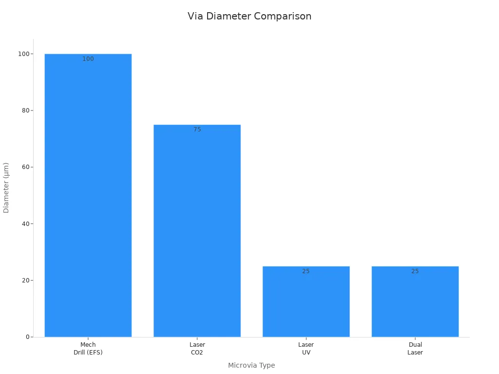
A comparison of drilling methods highlights how manufacturing choices affect cost and performance. Mechanical drilling works well for larger vias but becomes expensive and less efficient for small microvias. Laser drilling, especially with UV or dual laser systems, enables high throughput and smaller via diameters at a lower cost per via. The table below summarizes key manufacturing metrics:
Microvia Structure / Method | Via Diameter Range (µm) | Drill Rate (vias/sec) | Cost per 1,000 Vias (USD) | Notes |
|---|---|---|---|---|
Mechanical Drilling (with EFS) | Down to 100 | N/A | High below 150 µm | Best for large vias; tool wear increases cost for small vias |
Laser Drilling (CO2 laser) | >75 | Up to 65 | Below $0.60 | Efficient for FR4; limited for copper ablation |
Laser Drilling (UV laser) | Down to 25 | >100 | Below $0.50 | Produces smallest vias; high wall quality |
Dual Laser System (UV + CO2) | Down to 25 | High | Cost-effective | Combines speed and precision for high-volume manufacturing |
Manufacturers like LT CIRCUIT use advanced laser drilling to optimize cost and quality for HDI PCBs. This approach supports high-density connections and reliable performance while keeping costs manageable.
Performance Benefits
The performance benefits of microvias drive their adoption in next-generation HDI PCBs. Stacked microvias allow designers to maximize space and circuit density. This structure supports direct vertical connections through multiple layers, which improves signal integrity and reduces electrical path length. Staggered microvias distribute connections across the PCB, which enhances reliability and mechanical strength.
Technical studies show that microvia structure impacts reliability and performance. Key metrics include:
Failure rate plots reveal that microvia-in-pad structures may have a shorter lifetime compared to BGAs without microvias.
Failure rates depend on aspect ratio and the number of stacked vias.
Voiding in microvias is a critical failure mechanism that affects reliability.
Studies from IPC HDPUG and Sanmina provide detailed analysis on voiding and failure mechanisms.
These findings highlight the need for careful design and manufacturing to balance performance and reliability. LT CIRCUIT uses advanced quality control and material selection to address these challenges.
Laser and dual laser systems enable smaller via diameters and higher throughput, supporting the performance needs of compact, high-speed devices. Mechanical drilling remains a cost-effective choice for larger vias and low-volume production.
Application Scenarios
Application scenarios for microvias in HDI PCBs vary by industry and design requirements. In automotive electronics, a finite element modeling study shows that substrate composition and microvia location affect stress and failure risk. Designers must consider resin and fiberglass distribution to improve reliability and reduce failure costs in harsh environments.
Case studies in consumer electronics highlight the economic and technical benefits of both stacked and staggered microvias. Stacked microvias save space and improve signal integrity, making them ideal for smartphones and tablets where board space is limited. Staggered microvias offer higher reliability and simpler manufacturing, which suits multi-layer PCBs in telecommunications and industrial devices.
Manufacturers like LT CIRCUIT help customers select the right microvia structure for each application. Their expertise ensures that each PCB meets performance, reliability, and cost targets. This approach supports the cost-benefit analysis for advanced HDI PCBs, helping customers achieve optimal results in next-generation electronics.
Reliability and Performance
Signal Integrity
Signal integrity remains a top priority in HDI PCB design. Microvias help maintain signal integrity by reducing parasitic inductance and capacitance. Their small size limits noise coupling and crosstalk, which supports high-speed and high-frequency circuits. Unlike larger vias, microvias do not create stubs that cause signal reflections or electromagnetic interference. Advanced testing, such as the IPC TM-650 2.6.27A reflow test, reveals hidden defects in complex stacked microvias. This test simulates real assembly conditions and exposes fractures at metallurgical interfaces. These methods ensure that only robust microvias pass for high-reliability applications. LT CIRCUIT uses these industry-standard tests to guarantee signal integrity and reliability in every PCB.
Mechanical Robustness
Mechanical robustness is essential for HDI PCB reliability. Microvias face thermal and mechanical stress during manufacturing and operation. Staggered microvias show superior reliability under thermal cycling. The table below compares reliability between stacked and staggered microvias:
Parameter | Stacked Microvias | Staggered Microvias |
|---|---|---|
Failure occurrence | Fractures during reflow cycles | No fractures; withstand thermal strain |
Resistance change during reflow | Only 0.8% increase after six cycles | |
Open temperature range | Failures at 199.8°C to 249.3°C | No open events during multiple cycles |
Cycle-to-failure (CTF) | Many fail within first cycle | Up to 30+ cycles without failure |
Staggered microvias resist thermal expansion and maintain electrical integrity. Material selection and design choices, such as limiting stacking and using single-ply prepregs, further improve reliability and prevent reliability issues.
LT CIRCUIT Quality Standards
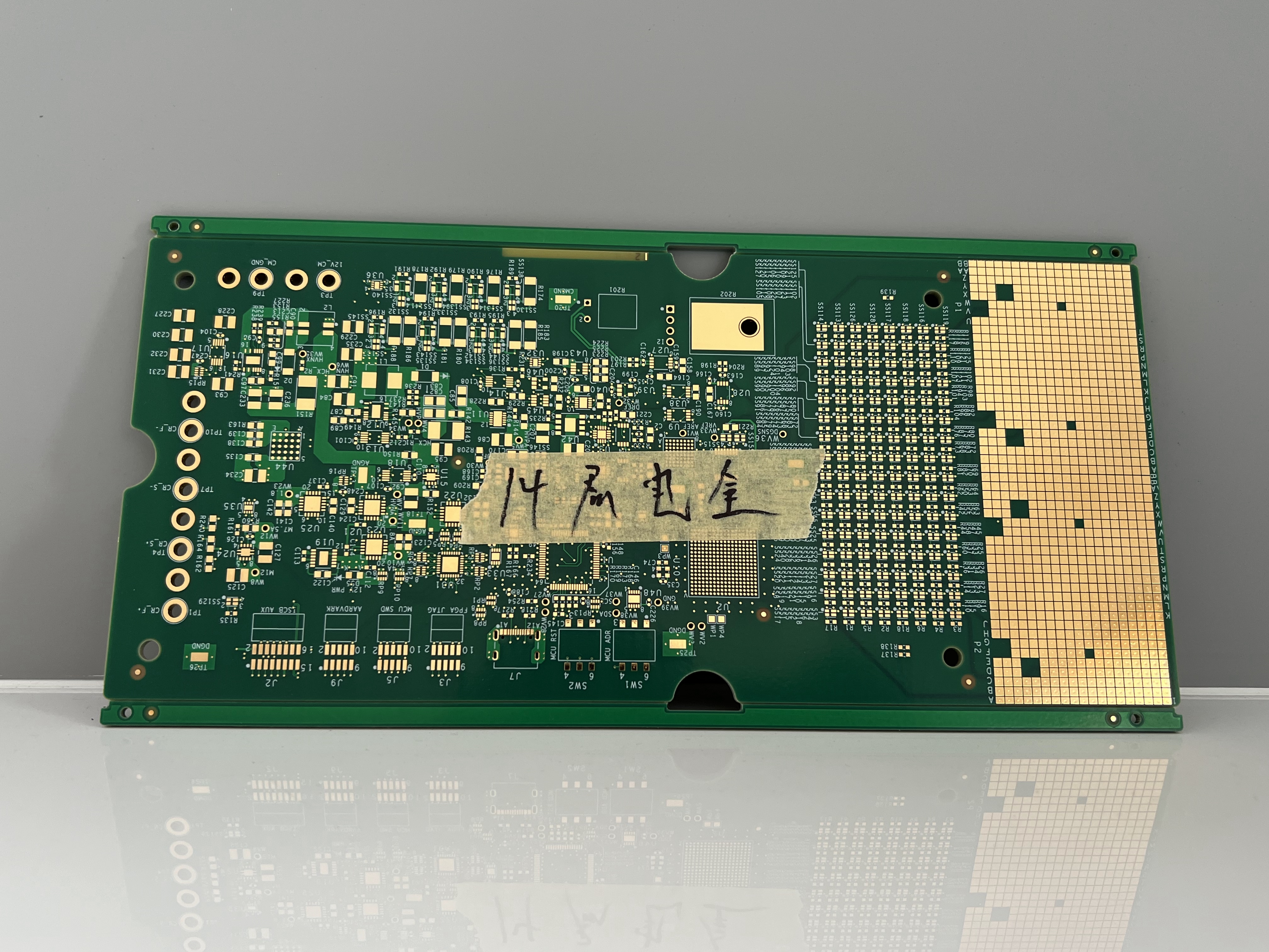
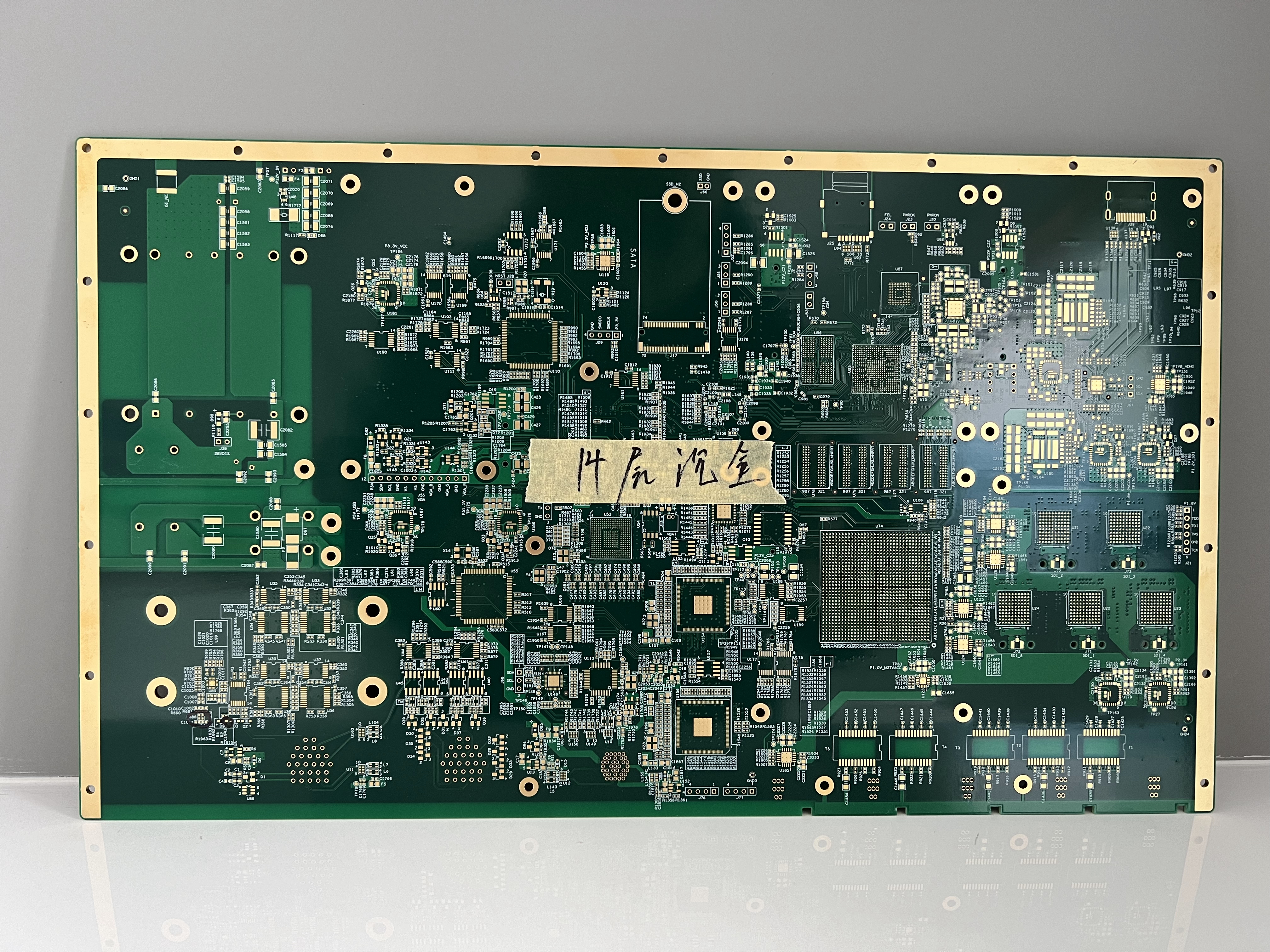
LT CIRCUIT sets high standards for HDI PCB reliability and performance. The company uses advanced machinery for precise drilling and placement of microvias. Real-time monitoring during production helps detect and correct reliability issues immediately. Quality control steps include engineer file checks, in-process quality control, and final auditing. Testing methods such as AOI, X-ray inspection, and functional tests ensure signal integrity and thermal reliability. LT CIRCUIT also uses back drilling to remove via stubs, which improves signal integrity. The company follows ISO 9001 certification and maintains a dust-free workshop with antistatic measures. Every PCB undergoes 100% electrical testing before shipment, ensuring full functionality and reliability for demanding applications.
Design and Manufacturing with LT CIRCUIT
Design Considerations
Engineers at LT CIRCUIT approach every HDI PCB project with careful design planning. They focus on layer stacking, microvia structure, and routing to achieve high-density interconnects. The design process starts with selecting the right microvia type—stacked or staggered—based on density, reliability, and cost. Layer count and sequential lamination play a key role in design, as minimizing layers reduces complexity and cost. Material selection is critical. LT CIRCUIT uses dielectric materials that ensure adhesion and thermal performance, and copper foils that support fine traces. Strict design rules guide line width, spacing, and aspect ratios. Signal integrity remains a priority, so engineers plan for shortest traces, controlled impedance, and proper ground planes. Environmental factors such as thermal management and mechanical stress resistance are also part of the design process.
Manufacturing Capabilities
LT CIRCUIT’s manufacturing capabilities support advanced HDI PCB solutions. The company uses advanced manufacturing techniques, including precise laser drilling for microvias as small as 0.1mm. Their process handles PCB thickness from 0.2mm to 6.0mm and copper weights from 0.5oz to 6oz. Engineers maintain tight control over line width and spacing, achieving 3mil/3mil for complex designs. The manufacturing team uses sequential lamination to build any layer count, supporting both simple and complex designs. Quality assurance is built into every step, with in-process checks and final audits. LT CIRCUIT’s manufacturing process supports applications in telecommunications, automotive, aerospace, and consumer electronics.
Customization and Testing
LT CIRCUIT offers a wide range of customization options to meet unique design needs. Customers can choose from various solder mask colors, silkscreen options, and surface finishes such as HASL, ENIG, Immersion Silver, and OSP. The company provides design optimization, material selection guidance, and stack-up recommendations. Testing is a core part of the manufacturing process. Every PCB undergoes Flying Probe Test and E-test to ensure electrical integrity. Engineers also offer troubleshooting and assembly support. This comprehensive approach ensures that each design meets strict quality and reliability standards.
Trends in HDI and Microvias
Industry Applications
Microvia technology has transformed the electronics industry by enabling smaller, more powerful devices. Engineers use microvias, which measure between 0.13 mm and 0.38 mm, to reduce PCB thickness and layer count. This approach allows for complex routing and high-density interconnections. As a result, designers can fit more features into compact products.
Microvia PCBs support critical systems in many sectors:
Telecommunication: High-speed networks and compact infrastructure rely on microvias for signal integrity.
Consumer Electronics: Smartphones, wearables, TVs, and gaming consoles use microvias to achieve miniaturization and advanced functionality.
Automotive: Electric vehicles and advanced driver assistance systems (ADAS) depend on microvias for reliable, high-performance electronics.
Medical Devices: Diagnostic equipment and wearable health monitors require microvias for precision and reliability.
Microvias also improve electrical performance by shortening signal paths and reducing unwanted capacitance and inductance. They help manage heat, which is vital for high-power, compact electronics.
A recent market report highlights key trends:
Aspect | Details |
|---|---|
Market Size & Forecast | USD 15.8 billion in 2024, projected to reach USD 24.4 billion by 2032 (CAGR 7.3%) |
Regional Trends | Asia-Pacific leads; North America and Europe focus on innovation and efficiency; emerging growth in Latin America and MENA |
Product Types | 1+N+1 HDI PCBs dominate; higher-order boards gain traction in advanced fields |
End-Use Industries | Consumer electronics, automotive, telecom, healthcare, industrial control |
Technological Advances | Laser drilling, sequential lamination, stacked vias, via-in-pad technology |
Future Outlook
The future of HDI and microvia technology looks promising. Manufacturers continue to adopt advanced processes like laser drilling and sequential lamination. These methods improve microvia formation and boost electrical reliability, especially for high-frequency circuits.
Miniaturization remains a key trend. Wearables, IoT devices, and 5G integration drive demand for thinner, more compact PCBs. Sustainability also shapes the industry. Companies shift toward green materials and energy-efficient manufacturing.
Market forecasts predict steady growth, with a CAGR of over 7% through 2031. Material innovations, such as high-frequency laminates and eco-friendly substrates, will further enhance performance and sustainability. Automation and collaboration among manufacturers, technology providers, and research institutions will accelerate progress.
Emerging applications in 5G, IoT, electric vehicles, and medical electronics will require even more advanced HDI microvia solutions. Regional growth in North America, China, Germany, India, and Japan will continue to shape the global landscape.
Engineers should weigh cost, reliability, and performance when choosing between stacked and staggered microvias. LT CIRCUIT delivers advanced HDI PCB solutions for every project. For high-density needs, stacked microvias excel. Staggered microvias suit multi-layer reliability. 📞 Contact LT CIRCUIT for expert advice and quality manufacturing.
FAQ
What is the main advantage of stacked microvias in HDI PCBs?
Stacked microvias allow engineers to save space and increase circuit density. This structure supports compact designs and high-speed signal transmission.
How does LT CIRCUIT ensure the reliability of microvia PCBs?
LT CIRCUIT uses advanced testing, strict quality control, and precise manufacturing. These steps help deliver reliable and high-performance HDI PCBs for every application.
Which industries benefit most from advanced HDI microvia technology?
Telecommunications, automotive, consumer electronics, and medical device industries use HDI microvia PCBs. These sectors require compact, reliable, and high-speed electronic solutions.
See Also
A Comprehensive Guide To Common Stack-ups In HDI PCBs
Unveiling Cutting-Edge Methods For HDI PCB Prototyping
Essential Design Tips For Manufacturing Reliable HDI PCBs