Essential Tips for Designing Heavy Copper PCBs for High Current
Heavy copper PCBs are important for high-power systems. They manage strong electrical currents and resist heat and damage. Many industries use them for key tasks like power supplies and electric cars. Good designs lower the chance of problems and handle heat well. This makes them dependable in tough conditions.
Key Takeaways
Heavy copper PCBs are important for high-power devices. They carry big currents and handle heat well, making them strong in hard conditions.
Picking the right copper thickness is very important. Thicker copper carries more current, handles heat better, and is stronger.
Using thermal vias and heat sinks helps control heat in heavy copper PCBs. Placing parts in the right spots stops them from overheating.
Understanding Heavy Copper PCBs
What Defines a Heavy Copper PCB
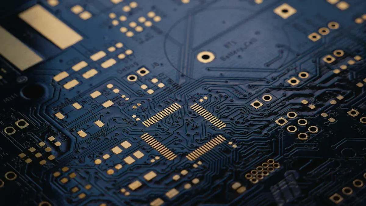
Heavy copper PCBs are special because they handle high current and heat. They have copper layers that are 3oz thick or more. This makes them great for tough jobs. Thicker copper helps carry more current and spread heat better. This ensures they work well in high-power systems.
Criteria | Description |
|---|---|
Copper Thickness | Heavy copper PCBs have copper layers 3oz thick or more. |
Current Carrying Capacity | They carry large currents, reducing heat and stress. |
Thermal Conductivity | Copper spreads heat well (401W/mK), keeping systems cool. |
Application Suitability | Used in defense, aerospace, and power systems for high-current needs. |
Key Advantages of Heavy Copper PCBs
Heavy copper PCBs have many benefits for high-current systems. They carry large electrical loads without overheating. Thicker copper spreads heat better, making them reliable and safe. These PCBs are also strong, so they last in tough conditions.
Advantage | Description |
|---|---|
Thicker copper layers help carry more current for high-power tasks. | |
Improved Thermal Management | Thicker copper spreads heat, preventing overheating and damage. |
Enhanced Mechanical Strength | Extra copper makes them strong and able to handle stress. |
Extended Lifespan | These features make them last longer and need less fixing. |
Applications in High-Power Electronics
Heavy copper PCBs are used in many high-power devices. For example, motor control systems use them to handle heavy electrical loads. Flexible PCBs with thick copper are great for power electronics, military tools, and electric cars. They are also key in medical devices and automation systems where reliability is critical.
Comparison: 1 oz vs. 2 oz Copper Thickness
1 oz.: Works for small to medium power needs.
2 oz.: Handles heat and heavy loads better.
Application: Motor Control Systems
1 oz. Copper Thickness: Good for small power but struggles with big loads.
2 oz. Copper Thickness: Manages heat and works well for heavy power needs.
Application: Flexible Printed Circuit Boards
Properties: Carries more current and spreads heat well.
Use Cases: Perfect for power electronics, military tools, medical devices, automation, and electric cars.
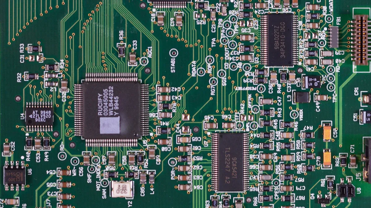
Essential Design Considerations for Heavy Copper PCBs
Choosing the Right Copper Thickness
Picking the right copper thickness is very important. Thicker copper improves how much current the PCB can handle. It also helps with heat control and makes the PCB stronger. Thicker copper lowers resistance, which is great for high-frequency uses.
Here are key points to think about when choosing copper thickness:
High Current Handling: Thick copper carries more current without overheating.
Improved Thermal Management: More copper spreads heat better, keeping parts cool.
Enhanced Mechanical Strength: Thick copper makes the PCB tougher and more durable.
Reduced Impedance: Extra copper lowers resistance, helping in high-current designs.
Increased Reliability: Thicker copper lasts longer and works better over time.
Design Flexibility: It allows complex layouts and supports higher currents.
Engineers use tools like ANSYS and SolidWorks PCB to plan copper thickness. The IPC-2152 standard also helps decide trace size based on current and heat rise.
Tip: Balance copper thickness with how easy it is to make the PCB.
Calculating Trace Widths for High Current
Trace width is important for handling high current safely. The IPC-2221 standard gives a formula to calculate trace width based on current and heat rise:
I = k × (ΔT^0.44) × W^1.0 × t^0.725
Where:
I: Current in Amps
ΔT: Allowed temperature rise in °C
W: Trace width in mils
t: Copper thickness in oz/ft²
k: A constant based on copper thickness
This formula helps figure out the right trace width for high current. Online tools make it easier by letting you enter current, heat rise, and copper thickness.
Note: Outer traces need less width than inner ones because they cool faster. Always check IPC standards for exact rules.
Handling Thermal Expansion and Stress
Heat expansion can weaken heavy copper PCBs in high-power systems. Matching copper and material expansion rates reduces stress from heat changes.
Evidence Description | Key Points |
|---|---|
CTE Matching Importance | |
High Aspect Ratio Vias | Thick plating helps reduce stress in tall vias. |
Glass Transition Temperature | Materials expand more above their Tg, causing extra stress. |
Stability of CTE | Stable expansion rates close to copper's are best for heat cycles. |
To handle heat stress well:
Pick materials with steady expansion rates.
Avoid tall vias unless reinforced with thick plating.
Use materials with a Tg that fits your needs.
Tip: Add thermal vias and heat sinks to spread heat and lower stress.
Ensuring Manufacturability with LT CIRCUIT's Help
Working with LT CIRCUIT ensures your PCB designs are easy to make and high quality. They offer full services and quick feedback to improve the design process.
Advantage | Description |
|---|---|
Fast feedback on your PCB design progress. | |
Comprehensive In-House Services | Full PCB assembly services for better results. |
High-Quality Standards | Reliable quality in prototypes and production. |
Quick Project Turnaround Times | Projects finished fast, saving time and money. |
With LT CIRCUIT, you get advanced tools to meet industry needs. Their focus on quality and innovation makes them a great choice for heavy copper PCBs.
Callout: Visit LT CIRCUIT's website to learn more about their services.
Best Practices for Thermal Management in Heavy Copper PCBs
Using Thermal Vias for Heat Dissipation
Thermal vias help remove heat in heavy copper PCBs. They let heat move easily from the top layer to the bottom. This keeps parts cool and prevents overheating. Place thermal vias under hot components for better cooling. Adding more vias improves heat removal but needs careful planning for space.
Factor | Description |
|---|---|
Thermal Via Sizes | Vias should be 0.2mm to 0.4mm wide for good heat flow. |
Placement | Put vias under hot parts to transfer heat well. |
Number of Vias | More vias help cooling but need space in the layout. |
Thermal vias give heat a quick way to escape.
They work best when placed under hot components.
Tip: Combine thermal vias with other cooling methods for better results.
Choosing High Thermal Conductivity Materials
Using materials that spread heat well is very important. These materials keep the PCB cool and safe. Copper layers in heavy copper PCBs act like heat sinks. They quickly move heat away from hot spots, protecting parts from damage.
Metal Core PCBs (MCPCBs) are great for high-heat uses. They have a metal core, like aluminum or copper, which spreads heat better than regular FR4. Copper-based MCPCBs are even better than aluminum ones for heavy current tasks.
Note: High thermal conductivity materials make PCBs last longer by stopping overheating.
Strategic Placement of High-Power Components
Where you place high-power parts affects cooling. Keep these parts away from sensitive areas to avoid heat problems. Don’t group hot parts together, as this creates heat spots.
Spread out high-power parts like processors and FPGAs. This helps heat spread evenly and avoids buildup. Align these parts with thermal vias or metal bases for better cooling. Good placement keeps your PCB cool and working well.
Tip: Plan where to put parts early to avoid heat issues later.
Incorporating Heat Sinks and Thermal Pads
Heat sinks and thermal pads are key for cooling heavy copper PCBs. Heat sinks move heat from the PCB to the air. Their design and material affect how well they work. Thermal pads improve the connection between parts and heat sinks for better heat transfer.
You can measure heat sink performance with this formula:
Tj = Ta + (Rja × Power dissipated)
Where:
Tj: Highest temperature of the part
Ta: Air temperature around the PCB
Rja: Resistance to heat flow from part to air
This formula helps check if your PCB stays cool enough. Use heat sinks and pads to keep your PCB running well and lasting longer.
Callout: Pick heat sinks and pads that fit your PCB’s cooling needs for the best results.
Advanced Techniques for High-Current Applications
Using Copper Busbars for Better Current Flow
Copper busbars help move high current efficiently in PCBs. They are strong and handle electrical loads well. Their design lowers inductance, cutting voltage spikes and noise. This keeps systems stable in high-power setups. Copper busbars carry large currents because of their size and quality materials. They also spread heat well, keeping parts cool and reducing the need for extra cooling. Their strength makes them last longer and resist damage from vibration.
Advantage | Description |
|---|---|
Lower Inductance | Reduces voltage spikes and noise by improving current flow. |
High Current Capacity | Handles large currents due to its size and material quality. |
Better Heat Management | Spreads heat well, keeping parts cool and lowering cooling needs. |
Strong and Durable | Resists wear and vibration, making it reliable for tough tasks. |
Tip: Add copper busbars to your PCB for better current flow and cooling.
Adding Terminal Blocks for Strong Connections
Terminal blocks make high-power connections easier in PCBs. They provide a safe way to connect wires and parts. To use them well:
Install them properly for better performance in high-current tasks.
Use tools and examples to design and install them correctly.
Terminal blocks are great for projects needing strong and reliable connections. They work well in many high-current applications.
Callout: Pick the right terminal blocks to improve your PCB’s reliability.
Multi-Layer Heavy Copper PCBs for More Power
Multi-layer heavy copper PCBs are great for handling high current. They stack copper layers to improve current flow and heat control. Each layer helps spread current evenly and keeps parts cool. These designs also allow for more complex layouts, so you can add powerful parts without losing performance. Multi-layer PCBs are strong and reliable, making them perfect for tough jobs like electric cars and factory machines.
Note: Multi-layer designs give you more options for high-current systems.
Why Choose LT CIRCUIT for Heavy Copper PCB Solutions
Expertise in High-Quality PCB Manufacturing
LT CIRCUIT has over 15 years of PCB experience. Since 2008, they’ve earned a strong reputation for quality. They serve customers worldwide, including the USA, Canada, Germany, and France. Their certifications meet IPC 610 Class 2 and Class 3 standards, proving their commitment to excellence.
Evidence Type | Details |
|---|---|
Established Year | Started in 2008 |
Industry Experience | Over 15 years making PCBs |
Global Reach | Trusted by customers in the USA, Canada, Germany, and France. |
Quality Control Certifications | Certified to meet strict IPC 610 Class 2 and Class 3 standards. |
Service Offerings | Full service from design to assembly. |
Customer Orientation | Focused on helping customers and ensuring satisfaction. |
Investment in Quality | Invests in top equipment and skilled workers for quality. |
Compliance Standards | Meets high industry standards for reliable production. |
Their expertise ensures your heavy copper PCBs are reliable and high-performing.
Customization Options for High-Current Applications
LT CIRCUIT knows every project is different. They let you customize heavy copper PCBs for your needs. Options include copper thickness, solder mask colors, and finishes like ENIG or HASL. These choices help create PCBs that work perfectly for your project.
Tip: Share your project details with LT CIRCUIT to find the best customization options.
Commitment to Innovation and Reliability
LT CIRCUIT focuses on innovation and reliability. They use advanced tools and skilled workers to stay ahead. This ensures you get modern solutions for high-current needs. Their PCBs are dependable, even in tough conditions.
Choosing LT CIRCUIT means partnering with experts who support your high-power projects.
Making heavy copper PCBs needs focus on copper thickness, trace size, and heat control. These factors must be optimized for strong and lasting performance.
Design Advice | Explanation |
|---|---|
Trace size for current flow | Use the rule: 500 circular mils per amp. For 5A, a 2oz copper trace should be 20 mils wide. |
Handling heat expansion | Control heat effects to avoid pad damage, board splitting, or bending. |
Balancing these with easy manufacturing leads to sturdy designs. Work with LT CIRCUIT for expert help with high-power projects.
FAQ
What is the thickest copper used in heavy copper PCBs?
Heavy copper PCBs can have copper layers as thick as 20 oz/ft². The exact thickness depends on your design needs and what your PCB maker can handle.
How can you find the right trace width for high current?
You can use the IPC-2221 formula or online tools. Enter the current, copper thickness, and temperature rise to get the correct trace width for your design.
Why pick LT CIRCUIT for heavy copper PCBs?
LT CIRCUIT provides top-quality manufacturing, custom options, and expert help. Their advanced tools create reliable solutions for high-power and high-current projects.
Tip: Reach out to LT CIRCUIT for advice on your heavy copper PCB design.
See Also
Essential Guidelines for Designing Effective PCB Circuit Boards
The Importance of Gantry Electroplating for Half-Hole PCBs
Utilizing Horizontal Copper Sinking Technology in PCB Manufacturing