ENIG PCB Manufacturing: Process, Quality Control & Testing Standards
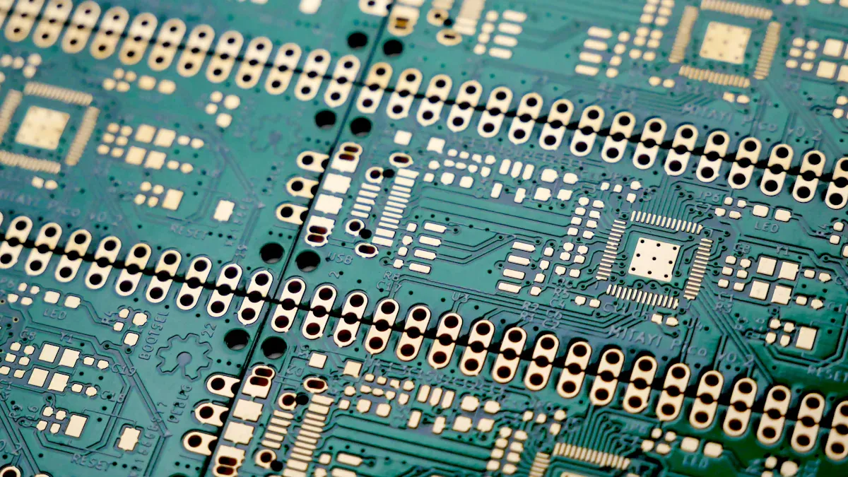
ENIG PCB manufacturing uses a dual-layer surface of electroless nickel and immersion gold to protect printed circuit boards. ENIG stands out as a preferred PCB surface finish in electronic devices. Empirical studies confirm the benefits of ENIG PCBs, such as enhanced solderability, corrosion resistance, and reliability, even in demanding environments. The surface finish maintains planarity and supports fine-pitch components, making ENIG essential for advanced electronic applications. Engineers choose this surface for high-performance printed circuit boards, recognizing the proven benefits of ENIG PCBs in modern manufacturing.
Key Takeaways
ENIG PCB manufacturing uses a precise process to create flat, corrosion-resistant surfaces that support reliable soldering and fine electronic components.
Strict quality control, including real-time monitoring and testing, ensures every ENIG PCB meets high standards for durability and performance.
LT CIRCUIT leads in ENIG PCB production by combining advanced technology, custom solutions, and strong quality management to deliver dependable, high-quality circuit boards.
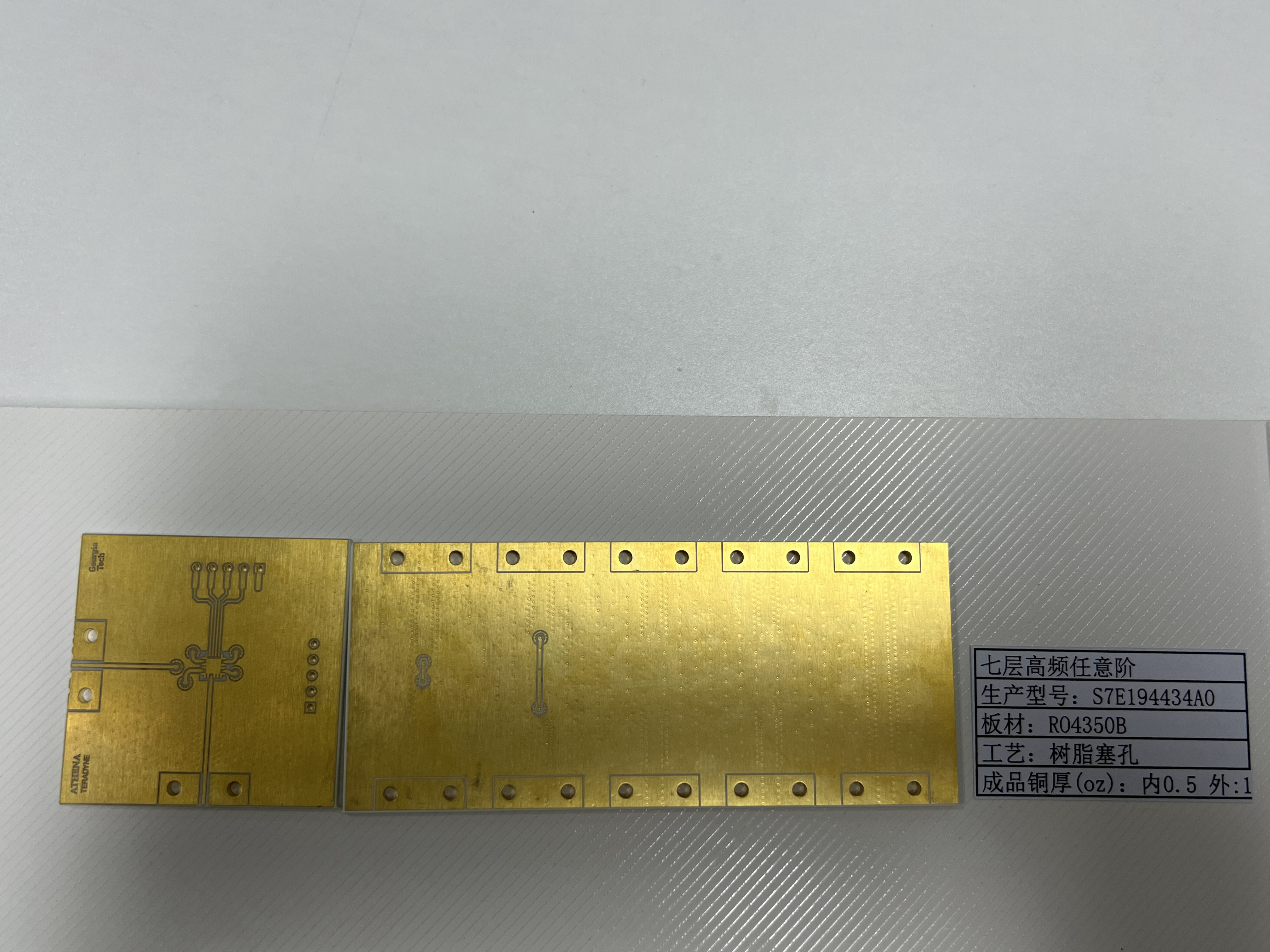
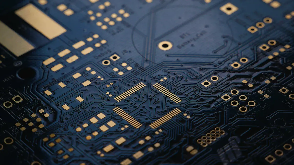
ENIG PCB Manufacturing
Process Overview
ENIG PCB manufacturing uses a precise sequence of steps to create a reliable and high-quality surface finish for printed circuit boards. The process begins with thorough cleaning and micro-etching of the copper surface. This step removes contaminants and prepares the board for further treatment. Next, the surface receives activation with a palladium catalyst, which ensures uniform nickel deposition.
The electroless nickel plating stage follows. In this step, a nickel-phosphorus alloy layer forms on the copper surface. The thickness of this nickel layer typically ranges from 2.5 to 6.3 micrometers, as outlined by IPC-4552 standards. The nickel layer provides a barrier that prevents copper diffusion and enhances corrosion resistance. The process uses controlled bath conditions, usually around 80°C, to maintain quality and avoid defects.
After nickel deposition, the process moves to immersion gold plating. Here, a thin gold layer, usually between 0.05 and 0.2 micrometers, forms on the nickel surface through a displacement reaction. This gold layer protects the nickel from oxidation and ensures excellent solderability. The gold also creates a flat, uniform surface, which is essential for mounting fine-pitch components during the PCB assembly process.
Quality control plays a vital role throughout the ENIG PCB manufacturing process. Technicians monitor metal ion concentrations and bath temperatures to maintain consistency. They use X-ray fluorescence spectroscopy (XRF) to verify coating thickness. Visual inspection and solderability testing confirm that the surface meets industry standards.
Technical articles highlight several advantages of the ENIG PCB manufacturing process. These include excellent surface planarity, reliable solder joints, and superior electrical conductivity. The process also ensures long-term protection against oxidation and corrosion. ENIG PCB manufacturing supports a wide range of applications, including consumer electronics, telecommunications, medical devices, automotive, aerospace, and defense.
Note: The ENIG process produces a flat, solderable surface that meets RoHS requirements and supports lead-free soldering. This makes it a preferred PCB surface finish for high-performance and environmentally compliant products.
LT CIRCUIT’s Approach
LT CIRCUIT applies industry best practices and advanced technology to every stage of the ENIG PCB manufacturing process. The company starts with rigorous surface preparation, using automated cleaning systems to ensure optimal copper surface quality. Their engineers carefully control each step of the process, from nickel deposition to gold plating, using real-time monitoring systems.
LT CIRCUIT follows strict quality standards, referencing IPC-4552 and IPC Class 3 Design Guide benchmarks. The team uses XRF analysis to measure nickel and gold thickness, ensuring each PCB meets precise specifications. They also conduct visual inspections and solderability tests at multiple points in the process.
The company’s approach to ENIG PCB manufacturing emphasizes reliability and performance. LT CIRCUIT’s process delivers PCBs with flat, uniform surfaces, robust solder joints, and high resistance to corrosion and thermal stress. These qualities are essential for advanced PCB assembly process requirements, especially in industries that demand high reliability.
LT CIRCUIT’s expertise in ENIG PCB manufacturing allows them to serve a diverse customer base. Their PCBs support applications in telecommunications, medical devices, automotive systems, and aerospace technology. The company’s commitment to quality and innovation ensures that each ENIG PCB meets the highest standards for performance and durability.
Key benefits of LT CIRCUIT’s ENIG PCB manufacturing process:
Flat and uniform surface for fine-pitch components
Excellent solderability and low contact resistance
Superior electrical conductivity
Long-term protection against oxidation and corrosion
Compatibility with lead-free and RoHS-compliant assembly
LT CIRCUIT’s dedication to process control and quality assurance sets them apart in the PCB manufacturing industry. Their ENIG PCB solutions provide the reliability and performance that engineers and manufacturers require for today’s advanced electronic products.
Electroless Nickel Immersion Gold Steps
Pre-Treatment
The electroless nickel immersion gold process begins with a critical pre-treatment stage. Technicians clean and micro-etch the pcb surface to remove oxides and contaminants. This step ensures the surface becomes electrochemically uniform, which is essential for consistent electroless nickel deposition. Removing oxide layers prevents poor adhesion and supports a dense, defect-free nickel layer. The pre-treatment process also forms an intermediate layer, reducing the potential gap between the base material and the electroless nickel deposit. This minimizes bimetallic corrosion and supports plating uniformity. Quality of nickel nucleation depends on this stage, influencing the overall reliability of the enig finish. Technicians monitor water contact angle, aiming for less than 10°, which confirms successful surface activation. They also measure phosphorus content in the electroless nickel deposit to ensure corrosion resistance. These benchmarks confirm the pre-treatment stage’s effectiveness in producing uniform, adhesive, and corrosion-resistant coatings in the enig process.
Metric | Value / Range | Significance / Interpretation |
|---|---|---|
Water contact angle | < 10° | Confirms successful plasma oxidation and surface hydrophilicity, validating the initial surface activation step. |
Ni content in final film | < 5 wt% | Indicates effective galvanic displacement of Ni by Au, ensuring film purity and quality. |
Sheet resistance | 3.1 ± 0.6 Ω/sq | Reflects the electrical quality and uniformity of the ENIG film. |
Resistance stability over time | Increase from 3.1 ± 0.6 Ω/sq to 6.2 ± 0.3 Ω/sq over 7 months | Indicates film stability and completeness of Ni displacement by Au. |
Nickel Deposition
After pre-treatment, the electroless nickel immersion gold process moves to nickel deposition. The electroless nickel bath deposits a uniform layer on the pcb surface. The industry standard for enig thickness in this step ranges from 3 to 6 microns, as specified by IPC-4552B. This thickness prevents copper diffusion and ensures robust solderability. Maintaining the correct enig thickness is vital for the reliability of the pcb. Technicians control bath composition, pH, temperature, and plating time to achieve optimal results. Automated process controls and real-time monitoring help maintain consistent electroless nickel quality. Quality control methods such as XRF thickness measurement and adhesion testing confirm that the electroless nickel layer meets manufacturing standards. The significance of enig thickness in this stage lies in its ability to provide a flat surface, excellent solderability, and compliance with environmental regulations.
Gold Deposition
The next step in the electroless nickel immersion gold process is gold deposition. The immersion gold layer forms through a displacement reaction, where gold atoms replace nickel atoms on the surface. Technicians must control this reaction to prevent hyper-corrosion, known as black pad. The recommended enig thickness for the immersion gold layer is 2–4 microinches, which aligns with IPC-4552A specifications. Maintaining this thickness ensures the surface remains solderable and corrosion-resistant. High-purity chemicals and stabilizers keep the plating bath quality high. Technicians thoroughly pretreat the copper surface to ensure good adhesion of both the electroless nickel and immersion gold layers. Regular quality checks, including XRF measurement and visual inspection, help detect defects early. The significance of enig thickness in the gold layer is its role in protecting the nickel and ensuring long-term reliability of the pcb.
Final Inspection
Final inspection is a crucial part of the electroless nickel immersion gold process. Technicians use visual inspection under bright lighting and magnification to detect soldering defects, incomplete wetting, and scratches. Automated Optical Inspection (AOI) systems check solder joint quality and component alignment. Automated X-ray Inspection (AXI) examines hidden solder joints and vias. Functional testing simulates real-world conditions to verify circuit performance. Electrical testing, such as in-circuit testing, detects opens and shorts. These inspection steps ensure only pcbs that meet stringent manufacturing standards proceed to shipment. Monitoring process capability indices and defect frequency helps maintain high reliability in the enig process.
Quality Control in ENIG PCB
In-Process Monitoring
In-process monitoring forms the backbone of quality control in ENIG PCB production. Technicians track each stage of the process to ensure that every board meets strict quality control standards. They use advanced tools to measure ENIG thickness, which is critical for both solderability and long-term reliability. X-ray fluorescence (XRF) analysis provides precise readings of nickel and gold layers, confirming that the ENIG thickness falls within the required range. Operators also monitor bath chemistry, temperature, and plating time to maintain consistency across all boards.
Quality control teams implement Statistical Process Control (SPC) techniques throughout manufacturing. These include process capability studies, control charts, and defect tracking. The goal is to keep process capability (Cpk) above 1.33, which indicates a stable and capable process. Regular data collection on yield rates, defect rates, and rework helps identify trends and supports continuous improvement. Personnel receive ongoing training to ensure they understand the latest process requirements and quality expectations.
Tip: Real-time monitoring and immediate feedback help prevent deviations in ENIG thickness, reducing the risk of defects and ensuring every PCB meets customer requirements.
Key in-process monitoring activities include:
XRF measurement of ENIG thickness at multiple points
Bath chemistry and temperature checks
Control chart analysis for critical parameters
Visual and automated optical inspections
Documentation for traceability and process review
Defect Prevention
Defect prevention is a proactive approach in ENIG PCB manufacturing. Engineers design the process to minimize the risk of common issues such as warping, corrosion, and poor adhesion. Empirical research shows that optimizing PCB design and controlling process parameters can significantly reduce deformation during reflow soldering. This reduces the chance of mechanical stress and related defects.
Environmental factors also play a major role in defect prevention. Studies have shown that humidity and contamination can lead to microporous corrosion and electrochemical migration on the ENIG surface. By maintaining a clean environment and using high-purity chemicals, manufacturers prevent these issues. Quality teams use Failure Mode and Effects Analysis (FMEA) to identify potential risks and implement corrective actions before problems arise.
Strict inspection of incoming raw materials ensures that only approved materials enter the process. Shelf-life management and traceability systems track materials from receipt to finished product. Automated inspection systems, such as AOI and AXI, detect surface defects, incomplete plating, and other anomalies early in the process. Continuous data analysis supports corrective and preventive actions, helping to maintain high reliability in every ENIG PCB.
LT CIRCUIT Quality Standards
LT CIRCUIT sets the benchmark for quality in ENIG PCB manufacturing. The company follows IPC-6012 and related IPC standards, which define acceptance criteria, testing methods, and process controls for high-reliability applications. Every ENIG PCB undergoes rigorous testing, including continuity, isolation, impedance, and thermal stress tests. For Class 3 applications, LT CIRCUIT adds extended thermal cycling, vibration, and outgassing tests to ensure the highest level of reliability.
The company’s quality management system covers every aspect of production. Document control, equipment calibration, and non-conformance handling form the foundation of this system. Personnel receive regular training and qualification assessments to maintain high standards. LT CIRCUIT also provides technical support, design optimization, and after-sales service to help customers achieve the best results with their ENIG PCBs.
The following table highlights LT CIRCUIT’s quality performance data for ENIG PCB production:
Parameter | Specification |
|---|---|
Material | Ceramic |
Surface Finish | ENIG |
Copper Weight | 1oz |
Minimum Hole Size | 0.2mm |
Minimum Trace Spacing | 0.1mm |
RoHS Compliant | Yes |
Maximum Operating Temp | 150°C |
Lead Time | 2 Weeks |
Layers | 2 |
Size | 10mm x 10mm |
LT CIRCUIT’s commitment to quality control ensures that every ENIG PCB meets or exceeds customer expectations. The company’s focus on precision, environmental compliance, and reliable delivery makes it a trusted partner for industries that demand the highest standards.
Testing Standards
IPC-4552A
IPC-4552A sets the standards of ENIG PCBs by defining the requirements for electroless nickel immersion gold plating. This standard specifies the thickness and uniformity for both nickel and gold layers. Manufacturers use quality control measures such as visual inspections, X-ray fluorescence (XRF) thickness measurements, and solderability testing. These pcb testing methods help ensure the reliability of the surface finish. The nickel underlayer plays a critical role in preventing defects like the black pad phenomenon. IPC-4552A does not provide comparative data on compliance across manufacturers, but it establishes a clear benchmark for quality in ENIG PCB production.
IPC-6012
IPC-6012 outlines the acceptance criteria and testing methods for rigid printed circuit boards. This standard addresses common failure modes in ENIG PCB testing, including delamination, plating voids, peeling gold, poor beveling, and electrical failures. The table below summarizes key failure modes and the corresponding pcb testing methods:
Failure Mode | Testing Method | Pass Criteria |
|---|---|---|
Delamination | Thermal Cycling | |
Plating Voids | Microsectioning | No voids detected |
Peeling Gold | Wear Resistance | 500+ rub cycles, no visible wear |
Electrical Failures | Electrical Testing | Continuity <1Ω, insulation >100MΩ |
These standards of ENIG PCBs ensure that each board meets strict reliability and performance requirements.
ISO Compliance
ISO compliance supports high-performance PCB testing by providing a robust quality management framework. Standards such as ISO 9001 and ISO 13485 validate the benefits of documented testing and process control. Manufacturers who follow ISO standards reduce risks, improve product reliability, and gain access to global markets. Key certifications include:
ISO 9001: Quality management for consistent product quality.
ISO 13485: Medical device quality requirements.
ITAR and DLA: Defense and security compliance.
Adhering to these standards increases customer confidence and ensures that every testing process meets international expectations.
ENIG PCB Challenges
Black Pad
Black pad remains one of the most discussed challenges in enig pcb manufacturing. This defect forms when the nickel layer develops a dark, brittle surface during the enig process. The result often leads to poor solderability and weak solder joint reliability. Industry data shows that black pad occurs in less than 1-2% of enig pcb production. However, even this rare occurrence can cause significant issues. Manufacturers may only discover black pad during assembly, which increases costs and delays. The defect creates an inferior solder-to-nickel connection, making it a costly problem to fix after manufacturing.
Black pad in enig pcb manufacturing is extremely rare, with an estimated occurrence rate of less than 1-2%.
The defect results in an inferior solder-to-nickel connection, often discovered during assembly, making it costly to detect and correct.
Solderability
Solderability is a critical factor for enig pcb performance. The enig surface finish provides excellent solderability, supporting strong solder joint reliability. Engineers value enig for its ability to create flat, uniform surfaces that help with fine-pitch components. However, several factors can affect solderability, such as surface contamination, improper storage, or excessive handling. These issues may lead to poor wetting, weak joints, or even open circuits. Manufacturers use strict process controls and regular testing to maintain high solderability standards. Reliable solderability ensures that each enig pcb delivers consistent solder joint reliability throughout its lifecycle.
Cost Factors
Cost factors play a significant role in the selection of enig as a surface finish. ENIG uses gold, which increases material and process costs compared to other finishes like HASL or OSP. A cost-benefit analysis shows that enig offers superior corrosion resistance, planarity, and long-term solderability, making it ideal for mission-critical applications. However, manufacturers must consider board size, layer count, and assembly complexity, as these influence the total cost. Prototype runs often have higher per-unit costs, while mass production benefits from economies of scale. Additional challenges, such as black pad defects, increased rework complexity, and thermal stress sensitivity, can also impact the economic evaluation of enig pcb solutions. Manufacturers balance these factors to achieve optimal solder joint reliability and performance.
LT CIRCUIT Advantages
Innovation
LT CIRCUIT leads the PCB industry with a strong focus on innovation. The company invests in advanced manufacturing technologies and materials. Their engineers develop new processes that improve ENIG surface finishes. LT CIRCUIT uses automated systems for precise layer control and real-time quality monitoring. This approach reduces defects and increases reliability. The team also explores new surface finishes and high-density interconnects. These efforts help customers achieve better performance in their electronic products.
LT CIRCUIT’s commitment to research and development keeps them ahead of industry trends.
Custom Solutions
LT CIRCUIT offers custom PCB solutions for a wide range of industries. The company works closely with clients to understand their unique requirements. Their engineers design PCBs with specific layer counts, trace widths, and surface finishes. LT CIRCUIT provides options for different solder mask colors and testing services. Customers can request prototypes or large production runs. The team supports projects from concept to delivery, ensuring each PCB meets strict quality standards.
Key custom solution features:
Flexible design options
Quick prototyping
Comprehensive testing services
Industry Recognition
LT CIRCUIT has earned recognition for excellence in PCB manufacturing. Industry groups and customers praise the company for its quality and reliability. LT CIRCUIT holds certifications such as ISO 9001 and ISO 13485. These certifications show the company’s dedication to quality management. Many leading electronics brands trust LT CIRCUIT for their PCB needs. The company’s reputation continues to grow as it delivers advanced solutions to global markets.
ENIG PCB manufacturing uses strict process steps and advanced testing to deliver reliable boards. LT CIRCUIT stands out by offering advanced solutions and strong process control. Companies should look for partners who value transparency and high standards. Choosing the right PCB provider ensures dependable performance in every application.
FAQ
What makes ENIG a preferred surface finish for PCBs?
ENIG offers excellent solderability, corrosion resistance, and a flat surface. Engineers choose it for high-reliability and fine-pitch electronic applications.
How does LT CIRCUIT ensure ENIG PCB quality?
LT CIRCUIT uses real-time monitoring, XRF thickness checks, and automated inspections. The team follows IPC and ISO standards for every production batch.
Can LT CIRCUIT provide custom ENIG PCB solutions?
Yes. LT CIRCUIT designs custom ENIG PCBs for various industries. The company supports different layer counts, finishes, and testing requirements.
For more details, visit LT CIRCUIT’s official website.
See Also
Step-By-Step Guide To The PCB Production Process
Essential Tips For Achieving Quality Control In PCB Production
Industrial Rigid PCB Production: Materials, Methods, And Standards
Understanding HASL Finish: Process And Quality In PCB Making
Key Quality Control Practices For Heavy Copper PCBs In Automotives