Advanced Testing Methods for HDI Bare Board Quality Assurance

HDI technology packs microvias and fine-pitch traces into tight spaces. These features make traditional testing methods insufficient for guaranteeing reliability. You cannot rely on standard visual checks or bed-of-nails fixtures alone. A strategic shift toward advanced, multi-layered testing methodologies is required to ensure hdi bare board quality. The hdi pcb market reflects this growing demand, with a projected compound annual growth rate of about 9.2% from 2023 to 2030. This article examines HDI-specific challenges and details advanced testing methods—flying probe, boundary scan, X-ray, and TDR—that address them. You will gain a practical roadmap for implementation.
Metric | Value |
|---|---|
Market Size (2023) | ~USD 4.2 billion |
Projected Market Size (2030) | ~USD 7.8 billion |
Projected CAGR (2023–2030) | ~9.2% |
Key Takeaways
Standard visual checks cannot catch hidden defects. Bed-of-nails fixtures fail on dense HDI boards. Advanced testing methods close the gap.
Flying probe testing reaches fine-pitch nets without a custom fixture. It suits prototypes and low-volume runs. It tests most nets sequentially.
Boundary scan testing uses JTAG cells behind BGA pins. It detects opens or shorts without physical probes. This method handles hidden connections.
X-ray inspection reveals voids inside buried microvias. 3D CT builds complete models. These methods inspect internal layers without destroying the board.
Time domain reflectometry sends pulses along traces. It reads reflected signals. This method pinpoints impedance mismatches in high-speed designs.
Design test points during layout. Follow HDI DFM rules for pad size and spacing. This step improves coverage and lowers costs.
Select AOI for fast checks. Use flying probe for prototypes. Choose X-ray for hidden joints. Match each method to volume and complexity.
HDI PCB Challenges in Quality Assurance
The HDI PCB manufacturing process builds circuits layer by layer, and each step introduces defect risks that standard boards rarely face. Laser drilling, sequential lamination, and copper plating all demand tight control. You must understand these challenges before selecting test methods.
Microvia Reliability and Defects
Voids and Incomplete Fill
Voids form when plating chemistry or laser parameters produce incomplete copper fill inside microvias. Stress concentrates around the void edge where copper is thinnest, which can cause intermittent connections after thermal stress. Reliable microvias require void-free plating, especially at the via bottom. A 100 μm microvia leaves almost no room for error during filling.
Interconnect Defects (ICDs)
ICDs occur when the copper-to-target pad connection fails. Rough via walls hinder plated copper adhesion, and resin smear blocks it entirely. Plasma etching removes debris before plating. Stacked microvias add risk because each layer must bond perfectly to the one below.
Fine-Pitch and High-Density Issues
Solder Bridging and Opens
Fine-pitch BGAs with pitch below 0.5 mm create narrow solder mask dams between pads. When these dams fail, solder flows across and creates bridges. Via-in-pad designs without non-conductive fill let solder wick into the via during reflow, starving the joint and causing opens. IPC-7095D recommends non-conductive fill for these designs.
Trace Width and Spacing Violations
Subtractive etching struggles below 50 µm because lateral etching removes a large percentage of conductor width. Semi-additive methods build copper only where needed, producing straighter sidewalls. This approach enables line widths below 50 µm for advanced HDI PCBs.
Signal Integrity and Impedance Control
Controlled Impedance in High-Speed Designs
High-speed nets need precise impedance. A 50-ohm single-ended trace typically runs 3.5 mil to 6.0 mil wide. Standard tolerance is ±10%, and tighter high-speed HDI demands ±7%. Trace width, dielectric thickness, and reference plane continuity all affect the result. You verify impedance through coupons and TDR measurement.
Crosstalk and Signal Loss
Tight routing increases crosstalk between adjacent traces. Split planes and large plane openings disrupt return paths and cause signal loss. Keep ground continuous under all controlled-impedance traces. Ground stitching vias within 1 mm to 2 mm of layer transitions reduce coupling.
Limitations of Standard Testing for HDI
Standard test methods served conventional PCBs well for decades. The hdi pcb manufacturing process now produces features far smaller than those methods can handle. You need to understand exactly where these tools fail before you invest in them.
Visual Inspection and AOI
Blind Spots with Microvias
Automated optical inspection captures surface images and compares them against a golden board. This works well for visible solder joints and surface traces. Microvias sit buried under layers or filled with copper, so the camera sees only a flat pad. You cannot detect a void or an incomplete fill through optical imaging alone. The hdi manufacturing process stacks these vias in sequence, which means a defect at layer three stays hidden after layers four through eight bond on top.
Human visual inspection faces the same wall. A 100 μm via opening offers no depth information under a standard microscope. Inspectors miss internal cracks and thin plating that only appear under thermal stress.
Electrical Testing (Bed-of-Nails)
Physical Constraints with Fine Pitch
Bed-of-nails in-circuit testing relies on spring-loaded pogo pins that contact test pads simultaneously. This approach demands at least a 50-thou (0.05 inch) test pad per net, ideally all on one side. HDI boards use narrower gaps, smaller pads, finer pitch packages, and higher connection density. The pads and spacing are far smaller than the probe grid requires, so the two are physically incompatible on high-density interconnects.
Fixture design also struggles when component pitch drops below 0.5 mm or when both sides carry SMD components. Gold-plated beryllium copper pins last 100,000 to 500,000 cycles, and pins in high-stress locations wear out sooner. You need a preventive maintenance program to keep contact resistance stable across thousands of test cycles.
Limitation | Explanation |
|---|---|
High initial cost | Custom fixture fabrication is expensive, with cost scaling by pin count and complexity. |
Longer development time | Mechanical design, wiring, and test program debugging can take weeks for intricate boards. |
Custom tooling and programming | Fixtures and programs are tied to stable designs, making them poorly suited for frequent revisions. |
Limited test points | Physical probe access restricts coverage in dense areas such as BGAs or shielded regions. |
The Gap Between Standard and HDI Complexity
Fixture-based electrical testing and flying probe systems diverge sharply on fine-pitch access, cycle time, and design-change impact. Bed-of-nails fixtures handle frozen designs at high volume with cycle times of 3 to 40 seconds per board. Flying probes need 30 seconds to 15 minutes per board, and that time scales with net count. A design revision forces a new fixture that costs hundreds to several thousand dollars and takes days to weeks to build. Flying probe systems recompile from the CAM netlist in hours.
Bed-of-nails in-circuit testing is limited by high initial fixture cost, longer development time for design and programming, the need for custom tooling and programming for each board revision, and limited test points due to physical access requirements. These factors make it less suitable for prototypes or low-volume runs, where flying probes offer more flexibility.
HDI and IC-substrate work often needs pitches in the tens of micrometers and controlled force so pads are not cratered. Flex and rigid-flex need planarization because a warped panel creates false opens that look like plating voids. Latent-defect and micro-short inspection modes matter on HDI work, where etch residue and micro-bridges are the dominant escape risk. Standard testing and inspection tools simply cannot reach these features.
Advanced Electrical Testing to Ensure HDI Bare Board Quality
Electrical testing must evolve when physical access shrinks. Three methods carry the load on dense HDI work: flying probe, boundary scan, and time domain reflectometry. Each one solves a different access problem.
Flying Probe Testing
How It Works for HDI
Flying probe testing uses movable probes instead of a fixed fixture. The system sequences tests point-by-point, which trades speed for versatility. This approach overcomes the need for dedicated test pads in many cases. The software compares electrical connectivity from accessible nodes against design data, so testing does not depend on a full pad array. Vias provide access to inner layers. An outer-layer via can confirm the presence and integrity of an inner-layer net without the probe ever touching the inner copper. When blind or buried vias block direct probing, the system uses the closest pin pad and confirms the connection through the netlist. CAD data, netlist, component positioning, and comparative data must all reference the same electrical node before measurements are trustworthy.
Flying probe typically tests 80 to 100 percent of nets sequentially, which is sufficient for most diagnostic needs. In high-density interconnects, flying probe access surpasses fixed pins because it can probe finer pitches. Initial cost stays low with no fixture required. Per-board cost runs higher, roughly $0.50 to $2 per board, because testing is sequential. Bed-of-nails achieves full parallel testing at a lower per-board cost for large runs, but fixture cost reaches $1,000 to $10,000 and fixed pins struggle to cover dense areas. Flying probe suits volumes under 100 boards and handles varying board sizes and geometries.
HDI DFM requirements still recommend adding test pads and access points. Even when flying probe can reach a net, a dedicated pad improves contact reliability and speeds up the test program.
High-Speed Probing Accuracy
Probe speed and positioning accuracy determine whether you catch micro-opens on fine-pitch nets. Modern systems move quickly between points and land with controlled force. This control matters on a bare HDI circuit board, where a cratered pad becomes a scrap unit. You should verify probe calibration against a known-good coupon before each production lot.
Boundary Scan (JTAG) Testing
Testing Interconnects Without Probes
IEEE 1149.1 boundary scan builds a four-wire test port and a chain of boundary scan cells around each JTAG-compliant IC. Each cell can drive or observe its connected package pin. No physical probe is needed. This method gives you electrical testing access to nets that no fixture can reach.
Detecting Opens and Shorts on BGA Nets
For interconnect testing, the EXTEST instruction shifts walking test patterns through the boundary-scan chain. A short between two BGA nets causes patterns to leak between cells. An open on a BGA ball causes the expected pattern to be missing at the corresponding cell. Because BGA balls hide under the package, the scan cell behind each ball is the only electrical access point. A missing joint or cold solder appears as an open on that net and is reported through the board-edge JTAG header. This makes boundary scan the strongest option for dense BGA areas on any hdi pcb.
Time Domain Reflectometry (TDR)
Pinpointing Impedance Mismatches
TDR launches a fast-rise-time pulse along a trace and observes the reflected signal. Discontinuities show up as reflections, and you can pinpoint them with resolution better than 1 inch. This technique locates impedance changes caused by opens, vias, stubs, or width variations. If the reflection coefficient equals zero, the trace has no discontinuities and the TDR results report no reflections. Impedance is an AC property and cannot be measured directly like resistance, so TDR provides a practical and accurate way to evaluate signal integrity in high-speed designs.
Verifying Signal Integrity
TDR characterizes differential transmission lines by driving the pair in odd, even, or differential modes and analyzing the resulting reflections. Modern instruments automatically compare incident and reflected amplitudes to provide direct readouts of impedance, reflection coefficient, and time for both common mode and differential impedance. You should validate controlled impedance coupons within the tolerance your design specifies. This step confirms that the hdi manufacturing process held trace geometry and dielectric thickness in range. TDR is preferred over frequency-domain methods for fast, repeatable impedance verification, and it directly supports the reliability requirements of high-speed HDI products.
Together, these three methods close the access gap that standard tools leave open. Flying probe reaches fine pitches, boundary scan reaches hidden BGA balls, and TDR reaches inside the transmission line itself. You need all three to ensure hdi bare board quality across the full range of HDI defects.
Advanced Non-Contact Inspection Methods
Non-contact methods let you inspect features that physical probes cannot reach. They also avoid the risk of cratering delicate pads during electrical testing. Three approaches dominate HDI work: 3D AOI, X-ray inspection, and laser scanning.
3D Automated Optical Inspection (AOI)
Measuring Via Fill and Surface Finish
Standard automated optical inspection captures flat images and compares them to a golden board. That approach fails on HDI features because it cannot measure height or depth. A 3D AOI system projects structured light or uses phase-shift techniques to build a height map of the board surface. This capability matters for via fill verification. You can measure whether conductive or non-conductive fill sits flush with the pad surface or sits below it. A recessed fill creates a weak solder joint later. The system also checks surface finish uniformity across fine-pitch pads. High-resolution optical imaging detects copper plating condition, surface scratches, drilling quality, resin residue, and fine edge definition. These checks confirm that the hdi pcb manufacturing process held tight control at each step.
X-Ray Inspection (2D and 3D/CT)
Inspecting Buried and Blind Vias
X-ray inspection penetrates hidden and hard-to-reach points. The machine emits radiation that passes through the board, and a detector captures the attenuated signal. This method examines blind and buried vias that no camera can see. A 2D X-ray produces a top-down image and suits high-speed first-pass screening. It resolves voids and bridging within standard acceptance criteria. However, 2D imaging lacks depth resolution for isolating blind or buried vias in HDI PCBs. A 2.5D laminography approach generates multiple angled views to separate overlapping via structures. This improves visibility compared to standard 2D. For full depth analysis, 3D computed tomography reconstructs hundreds of images into a complete volumetric model. This enables layer-by-layer examination of internal structures.
Analyzing Microvia Quality
3D CT provides a non-destructive way to analyze microvia quality and detect voids. The technique reaches resolution down to 1 micron and detects void areas as small as 2 percent. You can quantify void content against IPC-A-610 acceptance criteria. This level of detail matters for stacked microvias, where each layer must bond perfectly to the one below. A void at an inner layer stays hidden until thermal stress opens the connection. 3D CT separates overlapping BGA solder balls, verifies internal layer registration, and confirms microvia integrity that 2D imaging alone cannot resolve. The sequential lamination process builds these structures layer by layer, so a defect at layer three remains invisible after layers four through eight bond on top. X-ray inspection is the primary non-contact method for detecting buried via defects and microvia voids.
"2D X-ray suits high-speed inline checks for fine pitch overviews, while 3D CT excels at volumetric analysis of microvias and complex joints. Choose based on defect risk: 2D for routine, 3D for qualification."
Laser Scanning and Confocal Microscopy
High-Resolution Topography
Laser scanning and confocal microscopy provide excellent 3D surface visualization. A confocal microscope rejects out-of-focus light and builds a topographic map of the via opening. You can evaluate via opening profile, surface flatness, edge quality, surface deformation, and overall via morphology. These tools complement X-ray inspection because they capture surface-visible structures with high precision. A 3D measuring microscope inspects blind via surface quality and profile evaluation. It also verifies process consistency across panels. However, these optical methods have limited capability for internal structure evaluation. You need X-ray or cross-section analysis to see inside a via. Cross-sectioning offers excellent internal structure evaluation but destroys the sample. That makes it unsuitable for routine production inspection. Use it for process verification and failure analysis instead.
The table below summarizes how each non-contact method performs across key inspection dimensions.
Inspection Method | Surface Inspection | Internal Structure | 3D Surface Visualization | Best Applications |
|---|---|---|---|---|
Optical Microscope | Excellent | Limited | Limited | Routine visual inspection |
Cross-Section Analysis | Excellent | Excellent | Limited | Process verification and failure analysis |
X-ray Inspection | Moderate | Excellent | Limited | Internal structure evaluation |
3D Measuring Microscope | Excellent | Surface-visible structures | Excellent | Blind via surface inspection, profile evaluation, and process verification |
These methods are critical for verifying the hdi manufacturing process. They catch defects that electrical testing and inspection cannot reach. A combined approach gives you full coverage from surface to inner layers.
Implementing Advanced Testing in HDI PCB Manufacturing
You now know the methods. The next step is deployment. A tiered strategy balances cost, speed, and quality across your production flow.
Developing a Tiered Testing Strategy
Combining Standard and Advanced Methods
You assign each method to the stage where it delivers the most value. Automated optical inspection runs on every board after reflow because it is fast and repeatable. Flying probe testing suits prototypes and low-volume runs, where no fixture is required. X-ray inspection targets hidden or high-risk joints such as BGAs and QFNs. In-circuit testing handles volume production with a custom fixture. Functional testing provides final quality verification under simulated conditions.
Inspection Method | Best Suited Stage | Key Strength |
|---|---|---|
Automated Optical Inspection | After placement or reflow | Fast, repeatable, detects visible defects |
Flying-Probe Testing | Prototypes and low-volume runs | No dedicated fixture required |
X-ray / AXI | Hidden or high-risk joints | Reveals voids and hidden bridges |
In-Circuit Testing | Volume production | Fast for volume, detects shorts and opens |
Your decision criteria include board complexity, production volume, end use, component density, and the consequences of failure. A simple prototype may need only manual inspection and flying probe testing. A dense production assembly justifies inline AOI, selective X-ray, and dedicated electrical fixtures.
Design for Testability (DFT) and HDI DFM Requirements
Incorporating Test Pads and Access Points
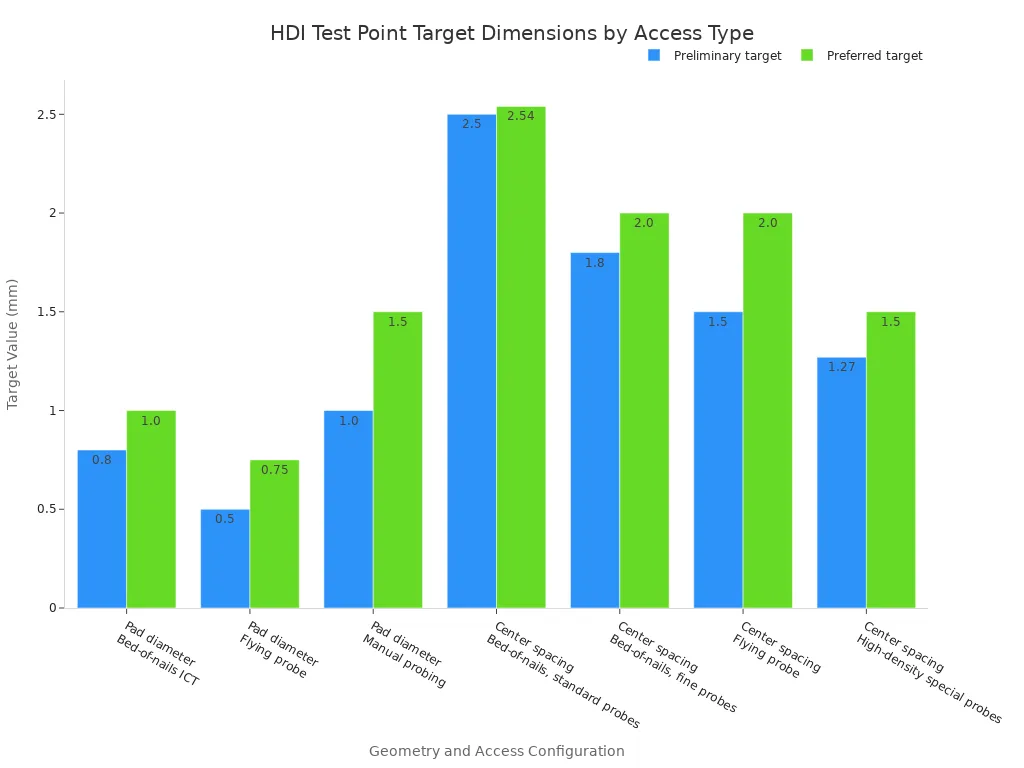
Test coverage is designed during layout, not purchased at the end. If a net has no accessible copper, pad, or test point, the tester cannot reach it. Adding a test pad during routing costs nothing because the copper is already on the net. Adding one after fabrication requires a full respin. Follow hdi dfm rules for pad geometry: use 1.0 mm flat copper pads with 2.54 mm spacing for optimal fixture contact. Place all test pads on the bottom layer to cut fixture costs. Match the test method to volume: flying probe for prototypes, bed-of-nails ICT for mass production. These hdi dfm requirements facilitate probe contact and improve test coverage across the hdi circuit board.
Temperature Cycling for Thermal Reliability
Simulating Extreme Temperature Variations
Temperature cycling exposes the hdi pcb to repeated thermal/mechanical shocks and reveals latent defects. The sequential lamination process builds microvias layer by layer, and each layer must survive expansion mismatch. IPC-TM-650 2.6.26A offers method examples: a default condition of 150 °C for 250 cycles, and a microvia condition of 190 °C for 250 cycles, both with a 10% resistance-change threshold. IPC-9701 defines its own conditions for solder joint reliability, with a preferred reference of 0 °C to +100 °C. IEC 60068-2-14 and JEDEC JESD22-A104 provide harsher profiles. Acceptance criteria include no open circuits, resistance change under 10%, and no visible cracking under 10x magnification. This reliability assessment confirms your hdi manufacturing process meets reliability requirements.
Thermal cycling subjects PCBs to repeated temperature extremes (e.g., -55°C to +125°C) to test for failures from thermal expansion mismatch. IPC-6012 Class 3 requires surviving 100+ cycles without interconnect failures.
Future Trends in HDI PCB Manufacturing
AI and Machine Learning in Defect Detection
AI analyzes test data and predicts failures before they reach final inspection. Modern line scan AOI platforms combine 8K–16K resolution optics with telecentric lenses and AI-powered defect classification. These systems inspect entire panels at micron level in seconds. They detect defects as small as 5–10 µm. High conveyor speeds produce no motion blur. This delivers 100% inline inspection coverage.
You feed captured image data into your MES and process-control loops. This enables closed-loop quality management and real-time yield optimization. Defect spikes trigger upstream process recalibration. AI models learn from historical defect patterns. They identify subtle anomalies that rule-based algorithms miss.
In-Line and Real-Time Testing Integration
Real-time online detection integrates into production lines for immediate feedback and process adjustment. In-line AVI systems inspect 30–60 PCBs per minute. Each inspection adds less than 5 seconds per PCB. These systems run 24/7. 3D in-line AVI with AI handles 01005 chips, fine-pitch BGAs, and micro-cracks on traces below 50 µm.
You stage inspection after solder paste, after component placement, and after reflow. A smartphone manufacturer replaced 10 manual inspectors with 2 in-line 3D AVI systems. Defect escape rate dropped from 1.2% to 0.05%. Inspection time per PCB fell from 18 minutes to 90 seconds.
Key in-line technologies include:
Technology | Real-time in-line role |
|---|---|
AOI | Multi-angle lighting and color filtering inspect solder joints and component placement. |
3D scanning | Laser or structured light detects height-related defects such as warping and solder-paste thickness. |
X-ray | Penetrates the board to inspect internal BGA balls, hidden wiring, and via/void defects; recommended with AOI for high-density boards. |
Real-time online detection | Integrated into production lines for immediate feedback and process adjustment. |
Testing for Advanced Packaging and 5G/6G
5G and 6G millimeter-wave designs push signal integrity requirements to new extremes. Vector network analyzers must cover DC to 67 GHz for 5G NR bands. Calibration uses on-wafer or coaxial standards. De-embedding removes test fixture effects. TDR impedance verification tightens to ±2Ω on critical nets. S-parameter measurements reach beyond 40 GHz. Near-field probing detects crosstalk between traces. Antenna testing verifies return loss and gain patterns.
Fabrication tolerances tighten as well. Trace width holds ±10% standard and ±5% critical. Layer registration requires ±25 μm. Via position requires ±20 μm for microvia arrays. Dielectric thickness holds ±5%. You rely on electrical testing to validate signal path consistency across these parameters.
6G preparation introduces terahertz materials such as glass substrates and LCP. Photonic integration supports extreme bandwidth. AI-driven design handles complex structures. Signal integrity simulation performs 3D EM modeling before production. This approach ensures your hdi manufacturing process produces reliable boards for advanced packaging.
HDI bare boards pack microvias and fine-pitch traces into spaces that defeat standard test tools. You need advanced methods to ensure hdi bare board quality. Flying probe reaches fine pitches without a fixture. Boundary scan tests hidden BGA nets without probes. X-ray and CT reveal voids inside buried vias. TDR pinpoints impedance mismatches along high-speed traces. Each method closes a specific gap.
A tiered strategy guided by HDI DFM requirements remains the cornerstone of quality assurance in hdi pcb production. Design test access early, combine inspection with electrical test, and validate thermal reliability. This approach keeps your hdi manufacturing process under control. As densities rise, that discipline separates reliable boards from costly field failures.
FAQ
When should you choose flying probe over bed-of-nails testing?
Flying probe suits prototypes and volumes under 100 boards. It needs no fixture and recompiles from CAM data in hours. Bed-of-nails wins for large production runs where cycle times of 3 to 40 seconds per board justify the fixture investment.
How does boundary scan test BGA nets that probes cannot reach?
IEEE 1149.1 boundary scan places a test cell behind each JTAG-compliant pin. The EXTEST instruction shifts patterns through the chain. A short leaks patterns between cells, and an open leaves an expected pattern missing. The board-edge JTAG header reports both.
What void size can 3D X-ray detect inside a microvia?
3D computed tomography reaches resolution down to 1 micron. It detects void areas as small as 2 percent. You can quantify void content against IPC-A-610 acceptance criteria. This matters for stacked microvias where a hidden void opens under thermal stress.
Why does TDR beat frequency-domain methods for impedance verification?
TDR launches a fast-rise-time pulse and reads reflections directly. You pinpoint discontinuities with resolution better than 1 inch. Modern instruments read out impedance, reflection coefficient, and time automatically. The method is fast, repeatable, and supports high-speed HDI reliability requirements.
Do you still need test pads when flying probe can reach fine pitches?
Yes. HDI DFM requirements recommend adding test pads and access points. A dedicated pad improves contact reliability and speeds up the test program. Use 1.0 mm flat copper pads with 2.54 mm spacing for optimal fixture contact.
What temperature cycling profile should you run for microvia reliability?
IPC-TM-650 2.6.26A offers a microvia condition of 190 °C for 250 cycles with a 10% resistance-change threshold. IPC-6012 Class 3 requires surviving 100+ cycles without interconnect failures. Acceptance also demands no visible cracking under 10x magnification.
Can AOI alone verify via fill quality on HDI boards?
No. Standard AOI captures flat images and misses height data. A 3D AOI system projects structured light to build a height map. It measures whether fill sits flush with the pad surface or sits below it. A recessed fill creates a weak solder joint later.
How do you balance cost and coverage in an HDI test strategy?
Assign each method to its highest-value stage. Run AOI on every board after reflow. Use flying probe for prototypes and low-volume runs. Target X-ray at hidden joints like BGAs. Reserve in-circuit testing for volume production with a custom fixture.
