How to make the electroplating filling holes of HDI PCB laser drilling more flat
Flat electroplating filling holes are important for HDI PCBs. They help the boards work well and last longer. Reverse pulse plating (RPP) stops paste from blocking holes. This lowers production steps and saves money. Methods like mSAP use very thin copper foil. This makes the surface even and smooth, which is needed for modern designs like via-in-pad and stacked vias.
Key Takeaways
Smooth electroplating holes help HDI PCBs work better. Signals move easily, making them more reliable.
Modern methods like pulse plating and laser drilling keep hole sizes even. This lowers mistakes and makes PCBs better.
Choosing good materials and improving plating steps makes HDI PCBs tougher and last longer. This saves time and money in making them.
Why Flat Electroplating Filling Holes Matter in HDI PCBs
Improving electrical performance and signal flow
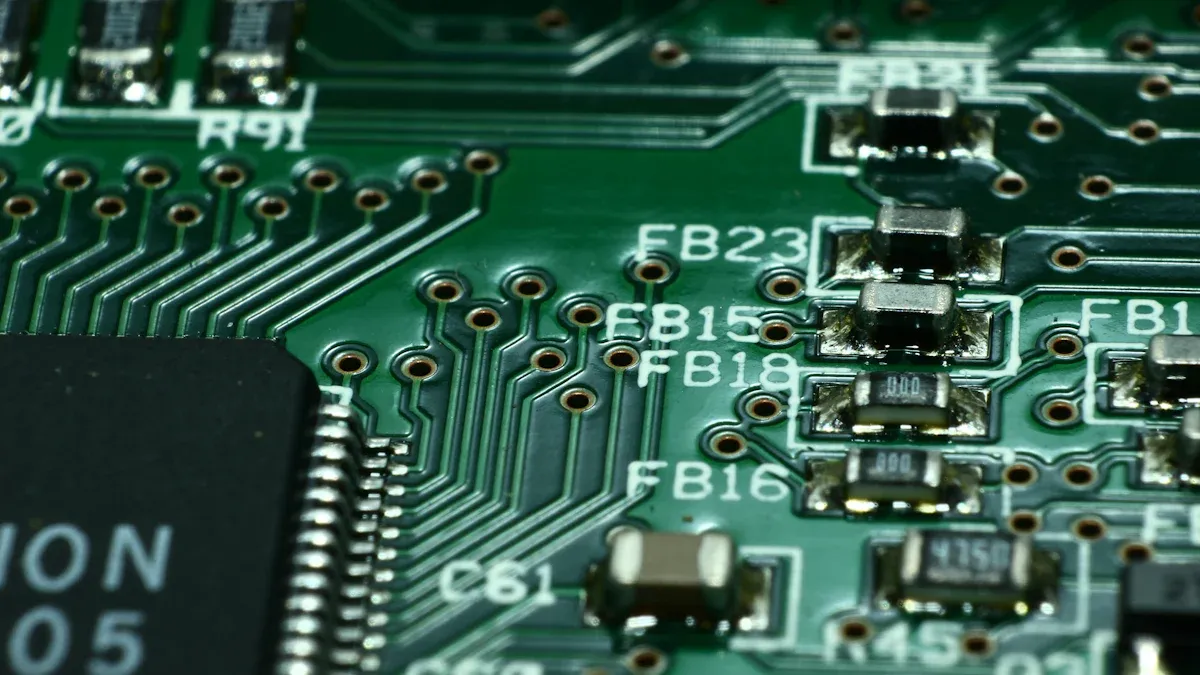
Flat filling holes help HDI PCBs work better. Uneven surfaces can block electrical signals, causing problems. Flat holes allow signals to move smoothly across the board. Copper-filled vias make connections stronger and stop air or liquid from getting trapped. This keeps signals clear and reliable. Flat holes are key for high-quality electronics. Resin-filled holes also improve electrical properties, helping the PCB work well under tough conditions.
Making PCBs stronger and last longer
Flat via filling makes HDI PCBs more durable. Filled vias create strong connections between layers, lowering the chance of damage from heat, stress, or moisture. The filler spreads out stress, stopping cracks or breaks. It also helps cool the board by spreading heat, which protects parts and makes them last longer. These features are important for high-performance PCBs.
Helping with advanced designs and smaller devices
Flat filling holes are needed for modern HDI PCB designs. Smaller, more complex devices need precise via filling. Resin or copper filling ensures holes are flat and reliable. Flatness reduces dimples in plated holes, improving PCB quality. New methods like semi-additive processes (SAP) make production faster while keeping holes flat. These techniques let you build small, dense designs without losing quality or strength.
Challenges in Achieving Flat Electroplating Filling Holes
Making flat electroplating filling holes in HDI PCBs can be tricky. The process is complex, and the materials used can cause problems. Knowing these challenges helps improve production and make better PCBs.
Uneven copper deposition during the electroplating process
Copper sometimes spreads unevenly during plating. This makes the filling bumpy and uneven. Thick copper layers in some spots can hurt fine lines and soldering. It may also trap solutions in the holes, making the PCB less reliable.
Problems like poor spacing between anode and cathode, weak stirring, or uneven current density cause this issue. For example, if the plating solution isn’t mixed well, copper spreads unevenly. Fixing these problems helps make the copper filling smooth and consistent.
Tip: Pulse plating works better than DC plating for thicker boards. It gives more control over copper spreading.
Challenge | Impact on Production |
|---|---|
Long plating time | Slower production |
High costs | More expensive |
Risk of entrapping solutions | PCB may fail |
Bad for fine lines and soldering |
Material inconsistencies affecting via filling
Different materials can change how well the holes fill. Some anodes add impurities to the plating solution, while others keep it clean. This affects how smooth the filling is.
Other things, like the rectifier’s accuracy and plating method, matter too. Precise rectifiers help fill small holes better. Pulse plating gives more control than older methods, making the filling smoother.
Parameter | Effect on Via Filling |
|---|---|
Some anodes add impurities; others keep the solution stable. | |
Anode-to-Cathode Spacing | Good spacing helps copper spread evenly. |
Stirring and Agitation | Mixing well stops uneven copper spreading. |
Current Density and Temperature | Lower values make filling smoother but slower. |
Rectifier Selection | Accurate rectifiers help with small holes and fine lines. |
Plating Waveforms | Pulse plating works better for thick boards than DC plating. |
Limitations of traditional PCB plating techniques
Old plating methods don’t work well for modern HDI PCB designs. They can’t fill holes with resin or copper precisely. This can leave dimples or gaps, lowering PCB quality.
Older methods also take longer and cost more. They aren’t good for making lots of PCBs quickly. Using new technologies and better processes can solve these problems and make flat filling holes easier.
Note: Automated plating systems and advanced solutions improve PCB quality and save time.
Solutions for Flat Electroplating Filling Holes in HDI PCBs
Optimized electroplating techniques and process parameters
To make smoother filling holes, improve the plating process. Change settings like current density, stirring speed, and temperature. These changes help copper spread evenly. Pulse plating works better than direct current plating. It spreads copper more evenly, especially on thick boards.
Laser drilling makes small holes in HDI boards. But high heat during drilling burns the edges. This leaves burnt material stuck inside the holes, making plating harder. Cleaning and removing burnt material before plating helps. Special methods for 2-HDI boards clean small holes better. These steps lower mistakes and waste, especially in complex 6-layer HDI designs.
Tip: Automated plating systems keep settings steady and improve production speed.
Selecting high-quality materials and additives for HDI PCBs
Picking good materials is key for strong HDI PCBs. Thin copper foils and special laminates improve electrical and heat performance. These materials also make the PCB stronger and last longer. Additives in the plating solution, like leveling agents, make holes smoother.
Material costs have gone up due to supply chain issues. Copper foil prices rose 18% in 2023. Special materials cost more but make PCBs more reliable. Using high-quality materials lowers defects and makes holes flatter.
Note: Work with trusted suppliers to get the best materials and additives for HDI PCBs.
Process adjustments to minimize uneven deposition
To avoid uneven copper spreading, adjust the plating process. Tools like COMSOL® 6.1 can find what causes unevenness. Changing cathode width and seed layer thickness helps. These fixes reduce uneven spreading from 20.326% to 12.257%.
Keeping the right space between anode and cathode helps copper spread evenly. Stirring the solution stops thick spots from forming. Accurate rectifiers make small holes and fine lines better. Pulse plating gives more control than older methods.
Tip: Check plating settings often to keep results steady and avoid problems.
Advanced Technologies for HDI PCB Via Filling
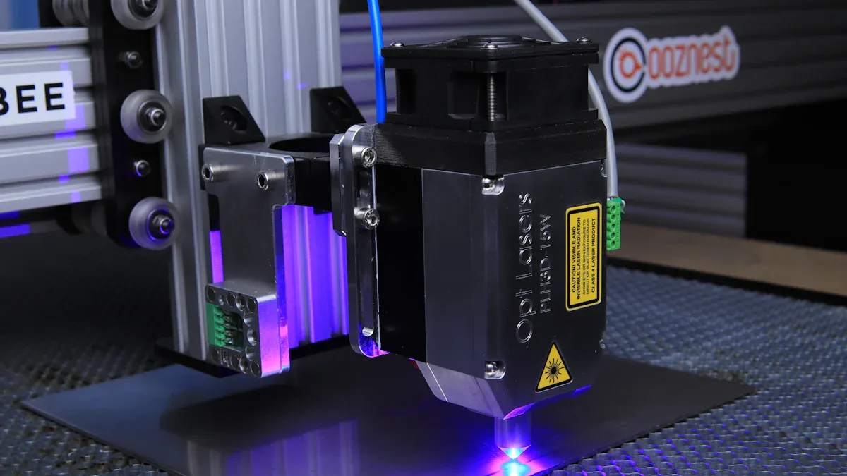
Precision laser drilling for consistent hole dimensions
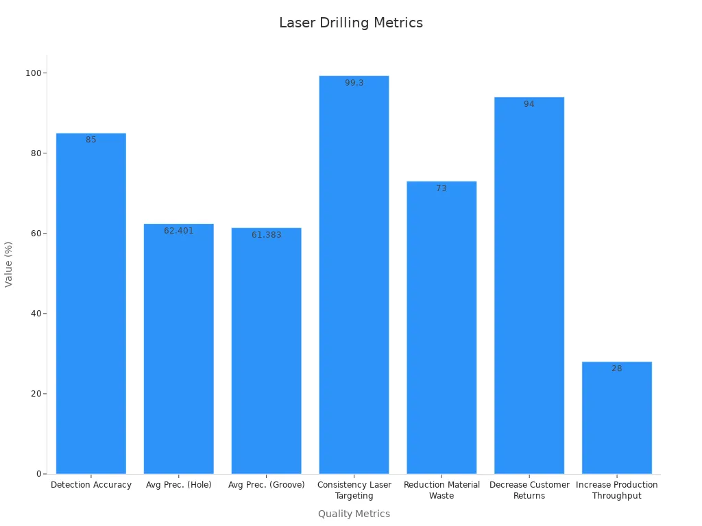
Laser drilling helps make holes in HDI PCBs the same size. This is important for keeping signals clear and the board strong. Using advanced lasers, you can make holes 99.3% accurate. This also cuts material waste by 73%, showing how precise and efficient laser drilling is.
Microvias in HDI boards allow more connections with fewer layers. But they need careful drilling to avoid mistakes. Laser drilling targets tiny areas with great accuracy, keeping errors small. This improves the quality of filled holes and speeds up production by 28%.
Automated plating systems for uniform electroplating filling holes
Automated plating systems make filling holes in HDI PCBs better. These systems use smart tools to adjust copper thickness as needed. They keep the thickness within ±0.1µm, making the filling smooth and even.
Features like selective plating save materials by 40%. Optical inspection finds mistakes as small as 10µm. These tools make HDI PCBs stronger and faster to produce. They also lower costs and improve reliability.
Feature | Description |
|---|---|
Submicron Accuracy | Smart tools adjust copper thickness to stay within ±0.1µm. |
Selective Plating | Only needed areas get plated, saving 40% of materials. |
In-Line Automated Optical Inspection | Finds mistakes as small as 10µm. |
Innovations in plating chemistry and equipment by LT CIRCUIT
LT CIRCUIT uses new ideas to make plating faster and cheaper. Switching from old cadmium plating to dry plating saves $1,000 daily per shift. It also cuts labor time by 30%.
LT CIRCUIT uses pulse-reverse plating to make smooth gold layers. This method keeps holes flat and strong. Their advanced tools help HDI PCBs last longer and work better. Using LT CIRCUIT’s solutions improves both quality and durability.
Process Type | Total Labor (Minutes) | Cost Savings per Day per Shift | Labor Cost Reduction |
|---|---|---|---|
Electroplated Cadmium | 107 | N/A | N/A |
Dry Plating | 76 | $1,000 | 30% |
Flat electroplating filling holes make HDI PCBs work better. Using improved methods and good materials gives smooth, strong results. These steps help make production faster and improve product quality. Check out LT CIRCUIT’s smart ideas to get great results and lead in electronics. 🌟
FAQ
What is the main benefit of flat electroplating filling holes in HDI PCBs?
Flat holes help signals move smoothly through the PCB. They also make the board stronger and last longer.
How can you achieve consistent hole dimensions in HDI PCBs?
Laser drilling makes holes the same size every time. It also saves materials and improves the PCB's quality.
Why should you choose LT CIRCUIT for HDI PCB solutions?
LT CIRCUIT uses smart plating methods and top materials. Their processes make flat holes that boost PCB strength and performance.
See Also
How Vacuum Two-Fluid Etching Machines Enhance PCB Precision
Impact of VCP on Copper Thickness Consistency in PCBs
Importance of Gantry Electroplating for Half-Hole PCB Copper
Utilizing Horizontal Copper Sinking Technology in PCB Manufacturing