How HDI Any Layer PCBs Are Designed and Manufactured
HDI any layer PCBs are a big step in electronics. They help make small, powerful devices using tiny holes and many layers. The HDI market is expected to grow from $20.63 billion in 2024 to $55.08 billion by 2033. This growth is due to the need for portable and smart gadgets.
Key Takeaways
HDI any layer PCBs help make small, strong electronics. They have smart designs with tiny holes and many layers to hold more parts in less space.
Picking the right materials is very important for HDI PCBs. Good materials make them work better, last longer, and save money.
Smart routing and placing vias improve signal strength and cut down noise. Putting similar parts together and keeping noisy ones away improves how devices work.
What Makes HDI Any Layer PCBs Unique?
Key Features of HDI Any Layer PCBs
HDI any layer PCBs are special because of their advanced design. They help create small, powerful electronics that regular PCBs cannot. Here are some features that make them stand out:
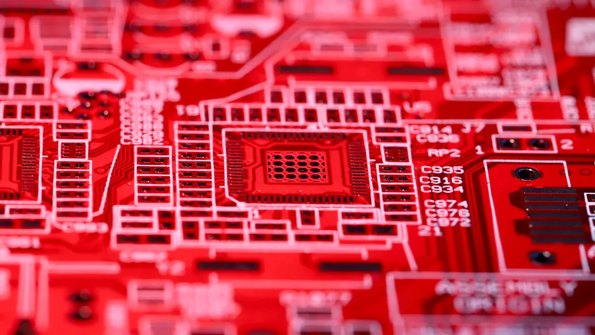
Higher Density of Microvias: These PCBs use tiny holes under 150 μm wide for connections.
Increased Layer Count: They often have 4 to 8 layers, sometimes over 10, unlike regular PCBs with 2 to 4 layers.
Enhanced Circuit Density: Thin lines (less than 100 μm) and close spacing fit more parts in less space.
Improved Signal Integrity: Shorter paths and special power layers reduce noise and improve signals.
Advanced Materials: These materials boost electrical and heat performance, making them reliable.
Metric | Description |
|---|---|
Enhanced Component Density | Tiny holes and thin lines allow more parts in small spaces. |
Higher Connection Pad Density | Fits more components in the same area. |
Increased Layer Count | Handles complex designs while staying thin. |
These features make HDI any layer PCBs perfect for modern, high-tech devices.
Applications in Advanced Electronics
HDI any layer PCBs are used in many advanced gadgets. Their small size and high performance make them important in different industries:
Application Area | Description |
|---|---|
Found in phones, tablets, and wearables needing small size and power. | |
Automotive | Used in smart car systems like ADAS and entertainment features. |
Telecommunications | Important for 5G networks, offering fast and stable connections. |
Medical Devices | Used in small, reliable tools for patient care and testing. |
Industrial Electronics | Helps in automation and smart factories with strong, efficient designs. |
These uses show how flexible and important HDI PCBs are in today’s technology.
Designing HDI Any Layer PCBs with LT CIRCUIT
Stack-Up Design and Layer Configuration
The stack-up design is very important for HDI PCBs. It affects how well the board works and how easy it is to make. Layers must be set up carefully to manage power, signals, and heat properly.
Here are some important things to think about:
Copper Thickness: Use thicker copper (1-2 oz) in core layers. This helps carry more current and improves power flow.
Via Technology: Use through-hole or buried vias in core layers. Make sure the drill size matches the layer thickness.
Plane Layers: Assign whole layers for power or ground planes. This improves power flow and reduces noise.
Signal Integrity: Keep signal paths short and avoid too many layer changes. This keeps signals clear.
Power Integrity: Use strong decoupling methods for power planes to prevent issues.
Manufacturing Considerations: Focus on layer alignment, microvia creation, and material choice to avoid problems during production.
At LT CIRCUIT, we follow IPC standards like IPC/JPCA-2315. These rules help us make reliable and high-performing HDI PCBs.
Material Selection for HDI PCBs
Picking the right materials is key for making good HDI PCBs. The materials affect how well the board works, lasts, and costs.
Here’s a look at common materials:
Features and Cost Details | |
|---|---|
High-Tg FR-4 Laminates | Good balance of performance and cost. Handles moderate heat well. |
Resin-Coated Copper (RCC) | Speeds up laser drilling but costs more upfront. |
Low-Loss Materials | Great for fast-speed uses. Use wisely to control costs. |
Halogen-Free Options | Meets eco-friendly rules. Costs more but saves money over time. |
At LT CIRCUIT, we match materials to your project needs. For example, we suggest high-Tg FR-4 for general use and low-loss materials for fast-speed designs. This ensures great performance without overspending.
Routing and Via Placement Techniques
Routing and placing vias are key steps in HDI PCB design. Good techniques save space, reduce signal problems, and improve board performance.
Follow these tips for better routing and via placement:
Group similar components together for easier routing.
Keep 4-8 mil spacing between traces and parts.
Place fast-speed parts first to shorten signal paths.
Use tools to check and fix design mistakes.
Avoid large footprints to save space.
Pick compact components to fit more on the board.
Match part sizes to avoid signal mismatches.
Keep sensitive parts away from noisy ones.
Use ground planes to protect important traces.
Put high-current parts near power planes.
Separate noisy parts on different ground planes.
Don’t place parts or vias between paired signals.
At LT CIRCUIT, we use smart design methods to make top-quality HDI PCBs. For example, we use microvias to connect layers, saving space and improving signals. Our design-for-manufacturability (DFM) approach also ensures designs are easy to produce, cutting costs and avoiding errors.
What It Does | Benefits | |
|---|---|---|
Micro Vias | Tiny holes link layers and save space. | Improves signals and makes devices smaller and lighter. |
Design for Manufacturability | Ensures designs match what manufacturers can build. | Avoids design problems, lowers costs, and ensures usability. |
Component Selection | Picks parts based on size and availability. | Reduces costs and saves space, boosting efficiency. |
Stackup Design | Affects how complex and costly manufacturing will be. | Good stack-up design makes production easier and avoids issues. |
By using these tips and strategies, you can design HDI PCBs that are small, effective, and dependable.
Manufacturing HDI Any Layer PCBs
Sequential Lamination Process
The sequential lamination process is key in making HDI PCBs. It bonds layers together to form a strong and compact board. This process helps create high-density connections for advanced electronics. Each cycle adds a layer, allowing complex designs while keeping the board sturdy.
To make this process better, reduce the number of cycles. Using two or three cycles lowers costs and improves reliability. Picking the right materials is also important. High-Tg materials (≥ 180°C) with low expansion reduce stress from heat differences. Spreading heat evenly across the board makes it last longer.
Evidence | Description |
|---|---|
Lamination Cycles | Fewer cycles, like 2-3, save money and improve reliability. |
Material Selection | High-Tg materials with low expansion handle heat stress better. |
Structural Stress | Even heat distribution reduces stress and makes boards stronger. |
By managing these factors, the lamination process can produce high-quality HDI PCBs.
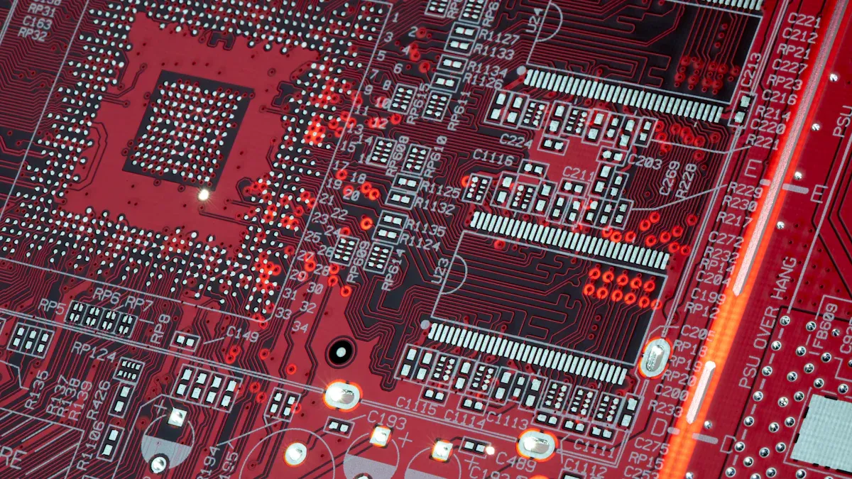
Laser Drilling and Microvias
Laser drilling is an important part of making HDI PCBs. It creates microvias, which are tiny holes connecting PCB layers. Microvias are needed for compact designs in modern electronics. Laser drilling is more precise than mechanical drilling and avoids defects.
Microvias allow complex circuits while staying reliable. Laser drilling reduces vibration, lowering the chance of mistakes. This method improves PCB quality and supports advanced designs.
Evidence Type | Description |
|---|---|
Manufacturing Defects | Laser drilling causes fewer defects than mechanical drilling. |
Design Complexity | Microvias help create detailed and complex circuit designs. |
Reliability Improvements | Laser drilling makes the PCB stronger and more dependable. |
Using laser drilling and microvias ensures accurate and reliable HDI PCB designs.
Plating and Surface Finishing
Plating and surface finishing are the last steps in making HDI PCBs. Plating adds conductive material, like copper, to microvias and traces. This improves signal flow and makes the board stronger.
Surface finishing protects the PCB and helps with soldering. ENIG (Electroless Nickel Immersion Gold) creates a flat surface for small parts. HASL (Hot Air Solder Leveling) is a cheaper option for regular boards. Advanced etching allows thin lines, keeping signals clear in fast designs.
Technique | Benefit |
|---|---|
Electroless Copper Deposition | Adds a conductive layer to microvias for better signal flow. |
Electroplating | Makes copper thicker for stronger boards and better signals. |
Advanced Etching Techniques | Creates thin lines for clear signals in fast designs. |
ENIG (Electroless Nickel Immersion Gold) | Provides a flat surface for small parts, improving soldering. |
HASL (Hot Air Solder Leveling) | A budget-friendly option for protecting regular boards. |
OSP (Organic Solderability Preservative) | An eco-friendly choice for fast signal designs. |
Choosing the right plating and finishing methods makes HDI PCBs last longer and work better.
Ensuring Reliability and Performance in HDI PCBs
Managing Heat and Keeping Cool
Managing heat is key to keeping HDI PCBs reliable. Too much heat can harm the board and shorten its life. Here are ways to handle heat better:
Use thermal vias to spread heat between layers.
Add heat sinks to cool high-power parts.
Pick materials like Isola Tachyon 100G for better heat flow.
Spot hot areas with thermal imaging and fix the design.
Make enclosures with vents for good airflow.
These steps help keep the board cool, so it works well even in tough conditions.
Keeping Signals Strong and Clear
Good signal quality is very important in HDI PCBs. Bad signals can cause data loss or system problems. Improve electrical performance by:
Grouping similar parts to shorten signal paths.
Keeping noisy parts away from sensitive ones.
Using short, straight traces to lower resistance.
Separating fast and slow signals to stop crosstalk.
Designing layers to balance cost and performance.
Using paired traces to cut noise and boost signals.
Ground planes also help reduce interference. A well-planned ground plane keeps signals steady and improves the board’s reliability.
Testing for Quality and Durability
Testing makes sure HDI PCBs meet high standards and work well. Manufacturers use many tests to check strength and performance. Common tests include:
Test Name | What It Checks |
|---|---|
Makes sure the solder mask handles heat and chemicals. | |
Acid and Alkali Test | Checks if the PCB can resist damage from harsh environments. |
Measures insulation between parts for steady performance. | |
Thermal Shock Test | Tests if the PCB can handle quick temperature changes. |
Temperature Cycling Test | Checks how the PCB holds up under extreme temperature swings. |
Thermal Storage Test | Ensures the solder mask stays strong during long storage. |
Careful testing, tracking, and records improve quality control. These steps make sure your HDI PCB is reliable and ready for different uses.
HDI any layer PCBs use smart designs and careful manufacturing. They are small, powerful, and work in many ways. These PCBs help make creative designs, send signals faster, and stay reliable. The table below shows their main benefits:
Benefit | Explanation |
|---|---|
HDI PCBs fit more parts in less space for smaller designs. | |
Better Performance | High-density circuits send signals faster and improve devices. |
Flexible Designs | Supports creative ideas and complex layouts with more features on one board. |
Strong Connections | Microvias and layers make connections stronger and reduce signal problems. |
Using HDI PCBs helps build smaller, better devices that work well in many areas.
FAQ
What is the main benefit of HDI PCBs?
HDI PCBs help make smaller and stronger devices. They hold more parts in tight spaces, boosting performance and saving room for tiny gadgets.
How do microvias help HDI PCBs work better?
Microvias link layers with great accuracy. This cuts down signal problems and keeps your device running smoothly and reliably.
Why does picking the right materials matter for HDI PCBs?
Good materials help HDI PCBs handle heat and fast signals. They also make the board last longer while keeping costs reasonable.
See Also
Uncover Cutting-Edge Techniques for HDI PCB Prototyping
Advantages of LDI Machines in Creating HDI PCB Circuits
Investigating Common Stack-Up Configurations for HDI Multilayer PCBs
How LDI Technology Impacts PCB Product Quality Significantly