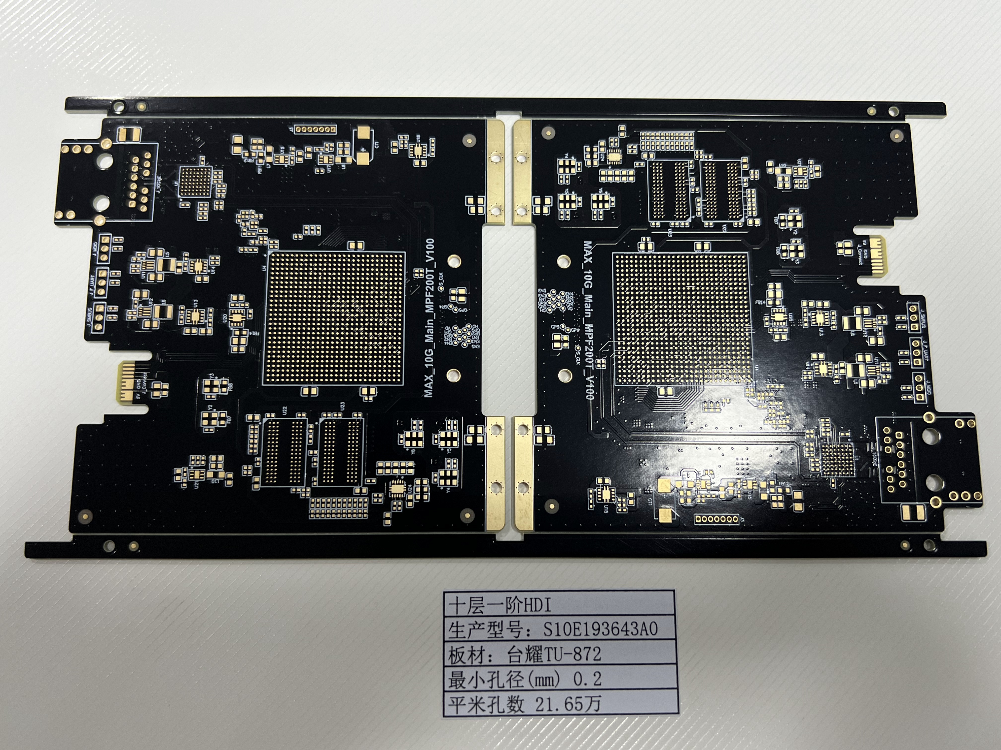
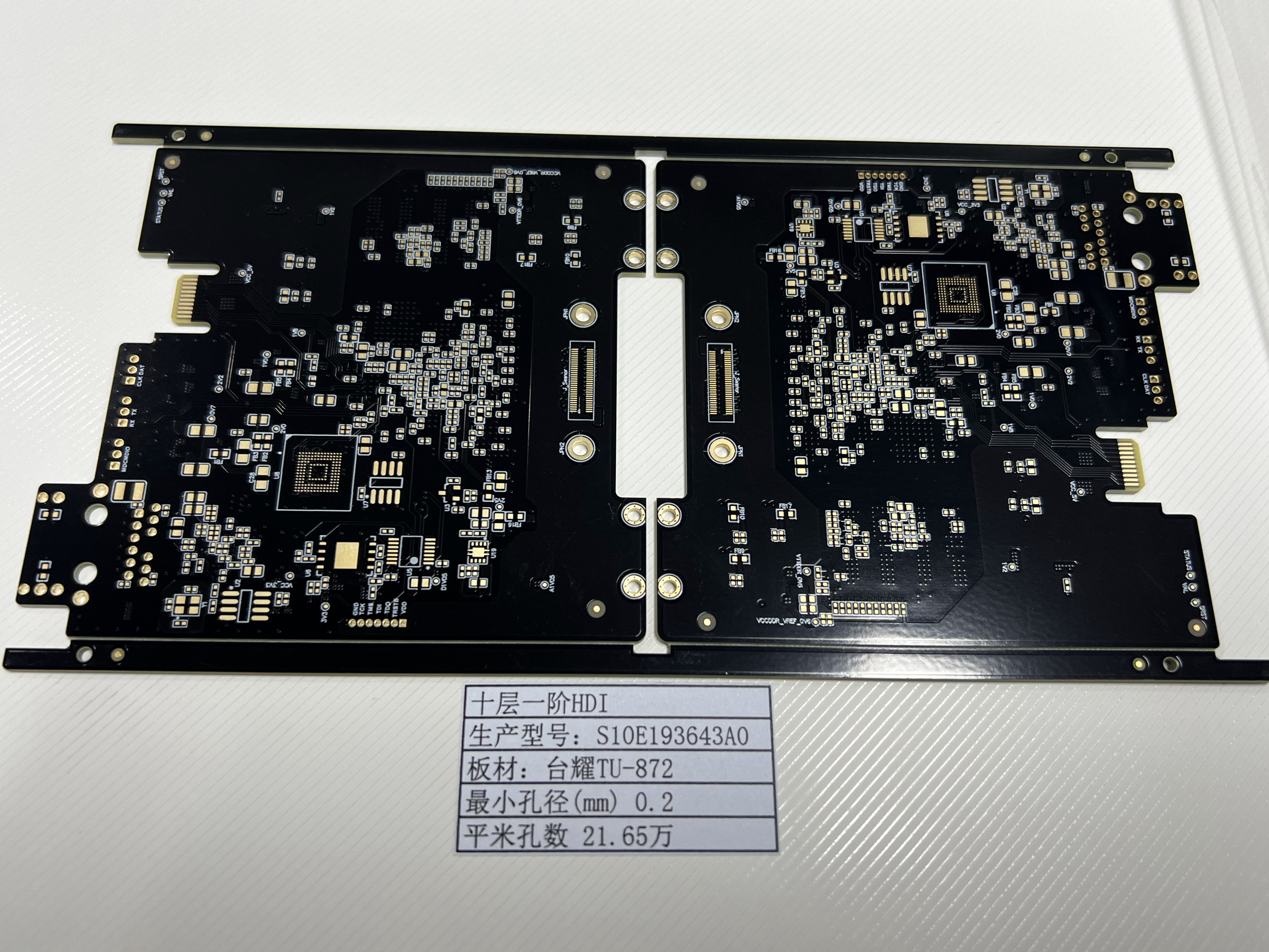
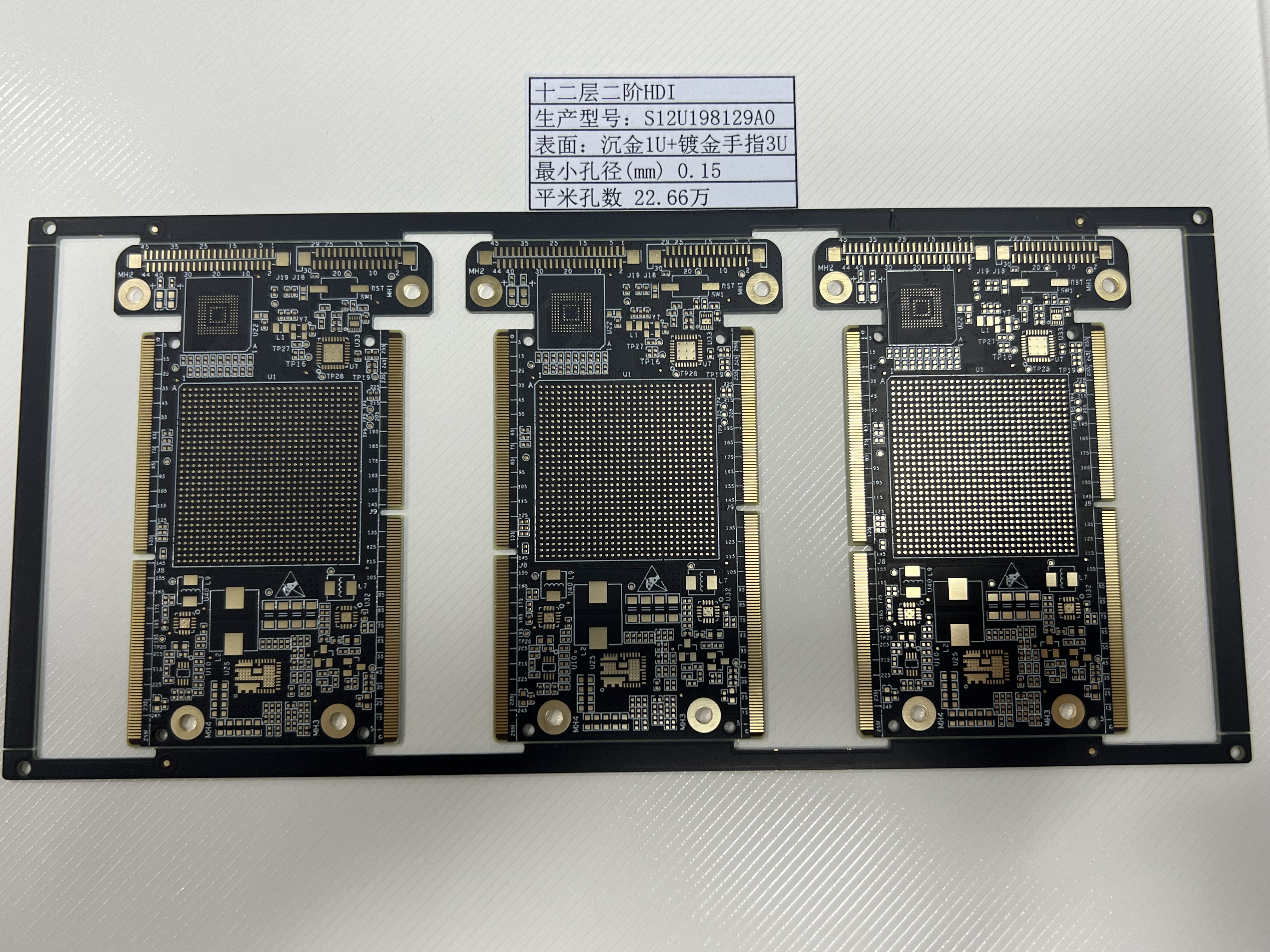
Optimizing HDI Layer Stackups for Large, Complex PCBs to Improve Signal Integrity and Thermal Management

Optimizing hdi layer stackups in big, crowded pcbs affects signal quality and heat control. You deal with problems like crosstalk, impedance control, and too much heat. Smart stackup design, picking the right materials, and using special via methods help keep signals strong in high-density pcb uses. Good optimization makes sure high-density interconnect and printed circuit boards work well.
Key Takeaways
Put high-speed signal layers close to ground or power planes. Use microvias to help signals stay clear and cut down on noise. Make ground planes solid and not broken. Use via stitching to lower electromagnetic interference. This also helps signals return better. Use thermal vias to move heat away from the PCB. Pick materials that spread heat well to keep the PCB cool. Balance the layer stackups so the board does not bend. This helps the PCB work better and last longer.
Signal Integrity in HDI Layer Stackups

Controlled Impedance
You must control impedance in every hdi pcb stackup to keep signals clear. High-speed signals work best on certain layer pairs. One layer goes up and down, the other goes side to side. This setup helps stop crosstalk and keeps signals on track. Put high-speed signal layers next to ground or power planes. This keeps impedance steady and helps signal integrity.
Dielectric thickness between signal layers and reference planes should be less than 10 mils (0.25 mm). This helps you reach the right characteristic impedance.
The layer stackup manager lets you set impedance profiles and figure out routing widths using material properties.
Setting up the hdi layer stackups and via start/stop layers early is important for impedance control and making the board.
IPC standards, like IPC/JPCA-2315 and IPC-2226, give formulas for wiring densities and microvia definitions. These standards help you make smart design choices.
Tip: The usual impedance tolerance for hdi pcbs is about ±15%. Some manufacturers can do tighter tolerances, like ±10% or even ±5%, if you ask early in the design.
To get these tolerances, you should:
Change trace width and thickness to hit the target impedance.
Pick dielectric materials with a steady dielectric constant.
Keep layers spaced right to lower crosstalk.
Put power and ground planes in good spots for a steady reference and fewer parasitic effects.
Use symmetrical or asymmetrical stackups depending on your large dense pcbs.
Use fewer prepreg types for better lamination.
Use sequential build-up processes, like laser drilling, for exact layer alignment.
Work with your manufacturer from the start to make sure your hdi pcb stackup meets all needs.
Power and Ground Planes
Power and ground planes are very important for signal integrity in hdi layer stackups. Always make a solid ground plane for signal return paths. This lowers EMI and voltage changes in large dense pcbs. Flat, unbroken ground planes under signal layers cut voltage drops and give short, low-impedance return paths. This setup stops ground loops and EMI.
Do not split ground planes. Splitting can mess up return current paths and add noise unless you use net ties or safety capacitors.
Use via stitching to link ground planes across layers. This gives low-impedance return paths and shields, making a Faraday cage at the board edges.
Keep power planes away from board edges. Let ground planes shield the edges.
Put decoupling capacitors close to power pins and connect them right to ground planes. This keeps power steady and lowers noise.
Note: Dedicated ground planes in hdi pcb stackup designs give a big conductive area with low impedance. This cuts noise, interference, and voltage changes, which is key for better electrical performance in high-density interconnect and large dense pcbs.
Microvia and Via-in-Pad Techniques
Microvia and via-in-pad techniques are needed to keep signal integrity in hdi pcb stackup designs. Microvias let you route signals in and out of fine-pitch parts, especially in boards with many layers. Via-in-pad lets you put vias right under component pads, saving space and helping miniaturization.
Microvias lower parasitic inductance by about ten times compared to regular thru-hole vias. This helps control impedance and lowers signal reflections.
Filled and capped vias stop solder from leaking during assembly, making the board more reliable.
Keeping the via aspect ratio low lowers signal reflections and helps electrical performance.
Smaller vias cut stray capacitance and inductance, making signal integrity better.
Flat filled vias under BGAs make solder joints more reliable.
Microvias and via-in-pad techniques also help you:
Lower layer count by removing through-hole vias, which lets you fit more routes.
Make electrical features better by lowering signal noise, EMI, and crosstalk.
Make it easier to break out BGAs, especially for pitches under 1 mm.
Help thermal management by letting vias be filled and capped.
Tip: Via-in-pad makes signal paths shorter and cuts signal distortion and reflections. This matters a lot in high-speed and high-frequency uses where signal integrity is very important.
Crosstalk and EMI Reduction
You must lower crosstalk and EMI in every hdi pcb stackup to keep signal integrity safe. Many strategies help you do this:
Use solid ground planes and switch power and ground layers in your stackup. This lowers crosstalk and makes return paths better.
Keep traces short and use differential routing for high-speed signals.
Place vias carefully so you do not mess up return current paths.
Use via stitching at board edges to make Faraday cages, which trap electromagnetic radiation.
Use embedded ground layers in multilayer hdi pcbs to shield and lower crosstalk.
Technique/Aspect | Description | EMI Shielding Effectiveness/Benefit |
|---|---|---|
Uses outer layers as ground planes, inner layers for power and micro-vias for signal routing | Outer ground layers act as excellent EMI shields, improving EMI/EMC compliance | |
Micro-vias and Buried Vias | Increase routing density and signal integrity | Reduces crosstalk and indirectly lowers EMI |
Via Aspect Ratios and Pad Sizes | Maintain optimal via dimensions (e.g., 5:1 for micro-vias) | Enhances routing density and signal integrity, aiding EMI control |
Ground Plane Placement | Assign ground to outermost layers | Provides low-impedance return paths and EMI shielding |
Layer Arrangement | Alternate power and ground layers, stripline configurations | Minimizes crosstalk and improves return paths, reducing EMI |
Routing Strategies | Via-in-pad, offset via-in-pad, dog-bone structures near BGAs | Increases routing density, reducing layer count and EMI sources |
Callout: Shielding materials like copper, aluminum, and ferrites work for different frequency ranges. Embedded ground layers and via stitching give strong EMI control in hdi layer stackups for large dense pcbs.
By using these strategies, you make sure your hdi pcb stackup keeps signal integrity and system reliability. You also get better electrical and electromagnetic performance, which is very important for high-density pcb and large dense pcbs.
Thermal Management in HDI PCB Stackup

Good thermal management in your hdi pcb stackup is very important. Large and complex boards get hot when you add more parts and power. Too much heat can break the board or make it work badly. The right hdi layer stack up, materials, and how you arrange layers help control heat and keep the board safe.
Thermal Vias
Thermal vias help move heat away from hot spots in hdi pcbs. They carry heat from parts to inside layers or ground planes. This spreads heat across the board. Put thermal vias right under hot parts to let heat escape fast.
Place thermal vias under or near hot parts, especially with exposed pads.
Use a grid pattern with spaces between 0.8 mm and 1.2 mm for good heat flow and strong boards.
Pick via sizes from 0.3 mm to 0.5 mm for easy making and good heat movement.
Fill or cover thermal vias with copper or special glue to help heat move and stop solder leaks.
Connect thermal vias to big copper ground planes or heat sinks to spread heat and stop hot spots.
Add more thermal vias to cool parts, but think about cost and space.
If you cannot add more vias, make them bigger or longer to help heat move.
If you plan where to put thermal vias in your hdi pcb stackup, you can lower part temperatures by up to 25°C. This keeps your board safe and helps it last longer.
Material Selection
Picking the right materials for your hdi layer stack up helps with heat control. Some board materials move heat better than others. Ceramic and metal-core boards move heat much better than regular FR4. These are good for boards that get very hot. High Tg materials help the board stay strong and not bend or crack when it gets hot or cold.
Material | Description and Usage | Thermal Management Properties |
|---|---|---|
Main board material; sticks well, not expensive | Moves heat well; used a lot in hdi pcbs | |
BT-Epoxy | Used in chip packages | Handles heat better than normal epoxy resin |
Cyanate Ester | Used in high-frequency boards | Low signal loss; handles heat well |
Polyimide | Used for bendy boards | Bends easily; handles heat well |
PTFE | Used in special boards | Good with heat; low signal loss |
You should also look at CTE and Tg when picking materials. If the CTE of your board and copper match, the board will not crack or bend. Using different materials together can help you save money, control heat, and keep signals clear.
Heat Dissipation Techniques
Special ways to move heat help keep big hdi pcbs cool. You can use built-in heat sinks, special pads, and smart layer setups to move heat away from hot spots.
Spread heat across the board with big copper areas and thermal vias.
Find hot parts and use pads or heat sinks to help move heat.
Do not put hot parts in the corners to stop small hot spots.
Put heat sinks or metal cores inside the board to spread heat better.
Use special pads, greases, or glue to help parts touch heat sinks better.
Put ground and power planes close to the top in your hdi layer stack up to help heat leave the board.
Tip: Try using thermal simulation tools to find the best places for parts, vias, and layers for good heat control in your hdi pcbs.
Stackup Symmetry
Stackup symmetry is important for both heat and strength in hdi pcb stackup design. A balanced hdi layer stack up stops the board from bending and spreads heat evenly.
Put prepregs and copper layers the same way on both sides of the board.
Make sure the top and bottom have the same amount of copper.
Use the same company for prepregs and core sheets to keep CTE the same.
Keep copper thickness even on the outside layers to stop stress and bending.
Make the stackup balanced to stop warping or cracks in vias.
A balanced stackup stops bending during making and helps with signal control. Putting ground planes next to signal layers and using thermal vias in smart spots gives good signal paths and easy ways for heat to leave. This is extra important in fast or thick hdi pcbs where heat and signals both matter.
Note: Always make sure your heat control plans also help with signal quality. The best hdi pcb stackup uses hdi pcb layer arrangement strategies that help both heat flow and clear signals.
PCB Design Optimization and Best Practices
Design Rules
You can make your pcb design better by following simple rules. First, pick how many layers you need for your circuit. Always add at least one ground plane and one power plane. This helps keep voltage steady and lowers noise. Use the same stackup on both sides to stop the board from bending. Keep the space between layers the same everywhere. Put ground or power planes between signal layers to stop crosstalk. Choose microvias, blind, and buried vias, but stay within what factories can make. Place ground planes close to signal layers for good return paths and strong signals. Put power planes in the middle and pair them with ground planes to lower loop inductance. Use the outside layers for fast signals to cut down on via jumps. Watch the thickness of the dielectric and pick materials that do not change much. This keeps signals clear. Test your stackup with a simulation before making the board. This helps you find problems early. Doing these things helps your board with both signals and heat.
Manufacturability
Making the board easy to build is very important. Complex HDI stackups can be hard to make. You might have problems like layers not lining up, holes being the wrong size, or the board bending. You can fix these by talking to your manufacturer often. Use high-Tg materials to help the board handle heat. Use laser drilling for microvias and special imaging for tiny lines. Fill vias with metal to make the board stronger. Check your design carefully to stop mistakes. Pick a manufacturer who knows how to work with small parts. Work together early to pick the right via sizes, trace widths, and spaces. This helps your board work well and not cost too much.
Parameter | Impact on Reliability | |
|---|---|---|
Inner Layer Clearance | Stops short circuits | |
Pad Size | ±20% | Makes soldering easier |
Hole Size | ±2-3 mils | Keeps connections working |
PCB Thickness | ±3 mils or 10% | Controls signals and heat flow |
Simulation and Validation
Simulation and testing help you make your pcb design better. Use tools like Ansys SIwave or HyperLynx to check fast signals, impedance, and EMI. For heat, use tools like Ansys Icepak to find hot spots and help heat move away. Connect these tools to your pcb layout software for quick checks. After you run simulations, check your board by looking at it and testing how it works. Do life tests to see how long your board will last. These steps make sure your hdi pcb stackup works in real life. By using both simulation and testing, you make sure your layer stackup helps with signals and heat.
Tip: Always use what you learn from simulations to make your design better. This helps you find and fix problems before you build the board.
You can make HDI layer stackups better in big, complex PCBs by doing these things: First, choose how many layers you need by using IPC standards. Next, use stackups that are the same on both sides and add microvias. Put ground planes right next to signal layers. Try out your design with a simulation before you build it.
Working with manufacturers early and using simulations helps your board work better, keeps signals clear, and controls heat.
FAQ
What is the main benefit of using microvias in HDI PCBs?
Microvias help you fit signal paths in small spaces. They make signals clearer and cut down on noise. They also help make the board smaller and stronger.
How do you choose materials for better thermal management?
You pick materials that move heat well and keep signals steady. This helps your board stay cool and keeps signals working right.
Can you use simulation tools for both signal and thermal analysis?
Yes. Simulation tools help you check signals and heat. You can find problems early and fix your HDI PCB design before making it.
See Also
Understanding Common Stack-Up Configurations In HDI Multilayer PCBs
Evaluating Costs And Benefits Of Advanced HDI Microvia Designs
Essential Design Factors For Reliable HDI High-Density Interconnect PCBs

