HDI Multilayer PCB Stackup Types and Their Unique Advantages
HDI multilayer PCB stackups are the foundation of modern electronics. Engineers choose hdi multilayer pcb stackups to achieve:
Compact device sizes, essential for smartphones and wearables
Enhanced performance through clearer signals and shorter routing paths
Increased reliability by reducing failure rates and supporting precise assembly HDI multilayer pcb technology enables circuits to be densely packed and operate at high speeds.
Key Takeaways
HDI multilayer PCB stackups help make devices smaller and faster. They also make devices more reliable. These stackups let you fit more parts in less space. They help signals move better inside the device.
There are different HDI stackup types like 1+N+1, 2+N+2, and ELIC. Each type has its own level of difficulty and how many parts it can hold. Each type also gives different performance. You can pick the right type for your device.
LT CIRCUIT makes special HDI PCB solutions for you. They use advanced ways to build them. They check quality very carefully. Their experts help you get the best results. This makes sure your device works well and lasts long.
HDI Multilayer PCB Overview
HDI Technology
HDI technology is very important for new electronics. LT CIRCUIT uses this advanced method to make high-density interconnect boards for many industries. HDI multilayer pcb technology lets engineers build small and powerful devices for today’s needs. The table below shows how HDI and traditional PCB technology are different:
Characteristic | HDI Multilayer PCB Technology | |
|---|---|---|
Design Complexity | Has many layers with complex patterns and circuits. Good for small, powerful devices. | Usually has one or two layers. Easier design for bigger devices. |
Component Density | High density with microvias, blind and buried vias. Makes smaller, lighter devices. | Lower density. Works for simple, low-density uses. |
Signal Integrity & Performance | Better because of shorter paths. Less signal loss and less electromagnetic interference. | May have trouble keeping signals clear at high speeds. |
Manufacturing Process | Uses laser drilling and special lamination. Costs more but works better. | Uses regular etching and lamination. Easier and costs less. |
Design Flexibility | More flexible with many layers and small size. Allows detailed designs. | Not as flexible. Best for simple uses without size limits. |
Thermal Performance | Gets rid of heat better because of materials and design. | Normal heat control. Not as good at moving heat away. |
Mechanical Strength | Stronger because of multilayer bonding and materials. | Normal strength. Not as tough under stress. |
Size | Smaller size is good for portable and tiny electronics. | Bigger size. Not great for very small devices. |
LT CIRCUIT’s skill in HDI gives strong, high-quality pcb products for electronics, cars, and telecom.
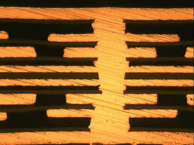
Stack-Up of HDI PCB
The stack-up of hdi pcb sets the electrical and mechanical features of each board. Engineers pick the best stack-up to control impedance, lower crosstalk, and keep signals clear. Good stack-up design also helps with EMI and heat control. Material choices like special dielectrics and copper foils help with fast signals and flexibility. Microvias and extra lamination steps make things harder but allow more parts and better reliability. LT CIRCUIT uses careful stack-up plans and advanced making methods to make sure each multilayer pcb meets high standards.
📈 The world market for HDI multilayer pcb is growing fast. This is because of more use in 5G, cars, and electronics.
HDI Stackup Types
1+N+1 Structure
The 1+N+1 structure is the easiest HDI stackup. It has one build-up layer on each side of a core. Microvias link the outer layers to the core. There are no stacked microvias in this design. This setup helps make small layouts and fit many parts close together. Engineers pick this stackup when they need small size and good performance.
Key features of 1+N+1:
One build-up layer on each side of the core
Microvias connect outer layers to the core
No stacked microvias
Typical applications include:
Smartphones
Tablets
Wearable devices
MP3 players
GPS systems
Memory cards
Medical equipment
This stackup helps make devices smaller and more advanced. It keeps signals clear by making the signal path shorter and lowering interference. LT CIRCUIT uses special lamination and microvia drilling to make 1+N+1 HDI multilayer pcb. Their way makes sure each pcb is reliable and lines up right.
2+N+2 Structure
The 2+N+2 structure has two build-up layers on each side of the core. This design lets engineers fit more paths and make harder circuits. It does not use stacked microvias but uses blind and buried vias. Engineers use this stackup for devices with more connections and smaller parts.
Key features of 2+N+2:
Two build-up layers on each side of the core
Blind and buried vias for interconnection
No stacked microvias
Increased routing density
Improved signal integrity
Enhanced power distribution
Greater design flexibility
Sequential lamination process
Precise layer-to-layer registration
Strict microvia size and plating control
Careful material selection for thermal and electrical performance
Typical applications:
Smartphones
PDAs
Game consoles
Digital cameras
Automotive electronics
LT CIRCUIT uses strong materials and advanced lamination to make 2+N+2 HDI pcb. Their process meets rules for impedance control and microvia strength. The company’s skill makes sure each multilayer pcb works well every time.
ELIC Stackup
ELIC, or Every Layer Interconnect, is the most advanced HDI stackup. In this type, every layer is an HDI layer joined by stacked, copper-filled microvias. This lets engineers send signals between any two layers, so they can fit more paths and parts. ELIC does not need through-hole vias, so there is more space for routing and parts.
Key features of ELIC:
All layers are HDI layers
Stacked copper-filled microvias connect every layer
Maximum routing density and design freedom
Advantages:
Shorter interconnect paths for low-loss signal transmission
Supports high pin-count and fine-pitch components
Enables ultra-thin pcb designs
Typical applications:
CPUs and GPUs
High-speed memory cards
Advanced mobile devices
High-performance computing systems
LT CIRCUIT makes ELIC stackups with careful lamination and microvia filling. Their process allows for very thin lines and tight layer matching, which is needed for hard, high-density designs.
Advanced HDI Stackups
Advanced HDI stackups include types like 3+N+3, 4+N+4, and any-layer HDI. These have more build-up layers and may use both stacked and staggered microvias. Engineers use these for the hardest jobs, where lots of connections and tricky paths are needed.
Structure Description | Typical Applications | |
|---|---|---|
1+N+1 | One build-up layer per side, no stacked microvias | Cell phones, MP3 players, GPS, memory cards |
2+N+2 | Two build-up layers per side, no stacked microvias | Smartphones, PDAs, game consoles |
3+N+3, 4+N+4 | Three or four build-up layers per side, may include stacked microvias | High-speed computing, telecom, military |
All layers are HDI, stacked copper-filled microvias | CPUs, GPUs, advanced mobile devices |
Key features of advanced HDI stackups:
Multiple sequential laminations
Stacked and staggered microvias
Fine line widths and thin cores
Enhanced signal layers and power distribution
Benefits:
Maximum component density
Superior signal integrity
Flexible routing for complex circuits
LT CIRCUIT follows IPC rules and uses a layer stackup manager to control impedance and routing. Their process supports thin traces, tight impedance, and advanced via types. The company’s skill in advanced HDI stackups gives strong performance for high-end electronics.
🛠️ LT CIRCUIT’s skills meet or beat industry rules. Their process supports hard HDI stackups, exact impedance control, and advanced microvia work. This lets them give high-quality pcb solutions for any job.
HDI Stackup Advantages
Space and Density
HDI stackups help save space and fit more parts on a board. Engineers can put many parts in small spaces. This is important for new devices like phones and tablets. Microvias and special layers let boards have lots of wires close together. This means products can be thinner and lighter but still work well.
Metric | Conventional PCB (Baseline) | HDI Stackup Improvement |
|---|---|---|
Component Density | 100% | |
Board Area | Baseline | Up to 40% reduction |
Routing Density | Baseline | 12X to 20X higher |
Layer Count | Up to 14 layers | Reduced to 8 layers (6 fewer) |
Routing Space (via blind vias) | Baseline | 30% more routing space |
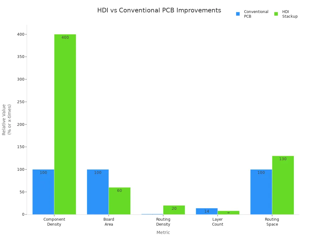
LT CIRCUIT uses strong materials like Megtron 6 and Panasonic R5775. These materials help the board work well, even when it is small. This makes hdi multilayer pcb good for phones, tablets, and other small electronics.
Signal Integrity
HDI stackups help keep signals clear in fast electronics. Engineers put signal layers next to ground or power planes. This helps signals travel safely and not bounce back. Controlled impedance design makes sure signals match at both ends. This stops signal loss and ringing.
Microvias and buried vias lower unwanted effects and keep signals strong.
Solid ground planes help stop signal problems and block interference.
Differential signaling and guard traces cut down on noise and crosstalk.
Shielding, like via stitching and metal shields, keeps EMI inside.
Thermal vias and good materials move heat away and keep signals steady.
LT CIRCUIT picks materials with low loss, like Panasonic RF775 and Shengyi SF305C. These materials help signals stay strong and fast. The company’s skill in stackup and material choice makes every pcb work well.
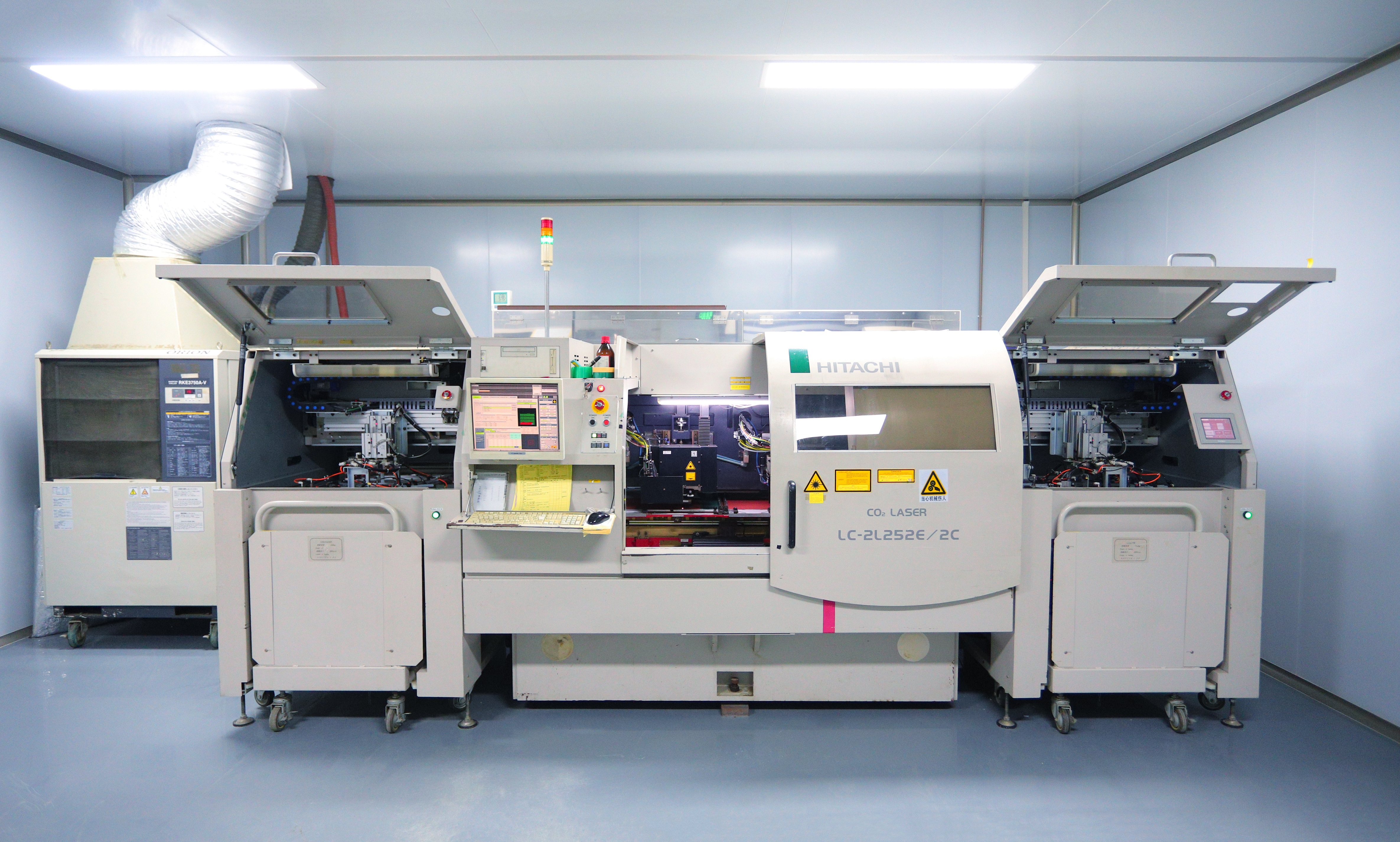
Manufacturing Flexibility
Making hdi pcbs gives more ways to design and build boards. LT CIRCUIT uses special steps to make this possible:
Laser drilling makes tiny microvias, as small as 20 microns. This helps fit lots of parts and connect layers easily.
Sequential lamination lets engineers add layers and drill microvias one after another. This helps make complex stackups like 2+N+2 with good alignment.
Via filling and plating make flat spots for parts and strong connections. This is important for via-in-pad designs.
Laser Direct Imaging (LDI) draws fine lines and copper shapes for detailed circuits.
Surface finishing like ENIG protects small parts and helps with soldering tiny pieces.
🛠️ LT CIRCUIT uses new materials and methods to make their hdi boards strong and work the same every time.
Engineers can pick from many stackup choices for different jobs. This flexibility helps with simple gadgets and also with big, powerful computers.
HDI Stackup Comparison
Key Differences
Engineers notice big differences between hdi stackup types. The 1+N+1 hdi stackup has one build-up layer on each side of the core. This type is the easiest to design and costs the least. The 2+N+2 hdi stackup has more build-up layers. This lets engineers fit more paths and make harder circuits. ELIC and advanced hdi stackups, like 3+N+3, have the most density and best signal quality. These types use stacked microvias and can connect any two layers.
Stackup Type | Routing Density | Signal Integrity | Manufacturing Complexity | Cost |
|---|---|---|---|---|
1+N+1 | Moderate | Good | Low | Low |
2+N+2 | High | Very Good | Medium | Medium |
ELIC/3+N+3 | Highest | Excellent | High | High |
Making more layers and using more microvias makes things harder and costs more. Simple hdi stackups are quicker and easier to make. Advanced hdi stackups need more steps and special machines. This makes them cost more and take longer to finish.
Tip: If you plan for easy building early, you can save money and keep your hdi pcb working well.
Best-Use Scenarios
Different hdi stackup types are best for certain jobs:
1+N+1 hdi pcb is good for things like MP3 players, GPS units, and simple medical devices. It saves money and still works well.
2+N+2 hdi pcb is used in smartphones, tablets, and car electronics. It helps make thin designs and fast devices.
ELIC and advanced hdi pcb stackups are for top uses like CPUs, GPUs, and smart car systems. These types give the best reliability and can fit the most parts.
Flexible-rigid hdi pcb designs are great for health monitors you wear and medical devices inside the body. They bend to fit shapes and keep strong connections.
LT CIRCUIT makes each hdi pcb stackup with strong materials and careful checks. Their boards work for industries that need small size, strong parts, and high performance.
Choosing LT CIRCUIT for HDI
Custom Solutions
LT CIRCUIT is special in the hdi market because they make custom solutions for each project. Their engineers talk with customers to design hdi multilayer PCB stackups that match what each person needs. They offer many ways to customize, such as:
Microvia aspect ratios and stacked microvias to fit more paths
Changing copper thickness for different power and heat needs
Impedance control to keep signals clear in fast hdi boards
Picking materials with low dielectric constant and low dissipation factor for better signals
Stackup designs that keep signal and power layers apart, and add thermal layers for strength
Choices for solder mask colors, silkscreen, and finishes like HASL, ENIG, and Immersion Silver
LT CIRCUIT engineers use advanced tools like laser drilling and sequential lamination. They can make complex hdi boards with up to 12 layers and very thin lines. Their team also helps with layout and picking the right materials, so each hdi board works well for things like 5G, medical, and aerospace.
Quality and Support
LT CIRCUIT checks quality at every step of making hdi boards. Their process uses:
Automated Optical Inspection (AOI) and X-ray checks to find problems
Real-time monitoring with AI tools to spot issues early
Skilled engineers watching each step of production
Following IPC rules for design and testing
Hard tests, like heating and stress tests
Checking suppliers for good raw materials
The company has ISO 9001, ISO 13485, UL, and CE certificates. These show they care about quality and trust. LT CIRCUIT also gives great customer support, helping from design to delivery. Their strong record makes them a trusted choice for hdi multilayer PCB solutions around the world.
Every HDI stackup type has its own special benefits. The 1+N+1 type works well for medium density boards. Advanced types like 3+N+3 give the best signal quality for hard designs. Picking the right stackup depends on signals, number of layers, and price. LT CIRCUIT’s team helps customers find the best and most reliable choice.
FAQ
What makes HDI multilayer PCB stackups different from standard PCBs?
HDI multilayer PCB stackups have microvias and extra layers. This lets them fit more parts on the board. They also help signals move better than in standard PCBs.
How does LT CIRCUIT ensure the quality of HDI PCBs?
LT CIRCUIT uses special tools to check their boards. They test each board with strict rules. Their engineers watch every step to make sure the boards work well.
Can LT CIRCUIT customize HDI stackups for unique project needs?
Yes. LT CIRCUIT can make custom stackup designs and pick different materials. They also offer many finishes. Their team talks with clients to meet special needs.
See Also
A Guide To Common Stack-Up Designs In HDI Multilayer PCBs
Evaluating Costs And Benefits Of Advanced HDI PCB Microvia Structures
The Process Behind Designing And Producing HDI Any Layer PCBs
Exploring Diverse Industry Uses For Multilayer Printed Circuit Boards
Unveiling Cutting-Edge Techniques For HDI PCB Prototyping Now