2+N+2 or Other HDI PCB Stackups Which Is Best for Your Project
Choosing the right HDI PCB stackup depends on your project’s needs. The hdi pcb 2 n 2 stackup works well for high-density interconnects in mobile, networking, aerospace, and medical devices. You can see how different projects benefit below:
Project Type | Description |
|---|---|
Mobile Devices | Ideal for smartphones and tablets requiring compact designs with high routing density. |
Networking Equipment | Benefits from signal integrity for high-speed interfaces like Ethernet or PCIe. |
Aerospace and Defense | Suitable for applications needing high reliability and performance with a higher layer count. |
Medical Devices | Compact designs for wearable or implantable devices balancing miniaturization and reliability. |
LT CIRCUIT guides you to the best stackup for your requirements.
Key Takeaways
The 2+N+2 HDI stackup is ideal for compact devices, offering high routing density and strong signal integrity.
Choosing the right HDI stackup requires balancing design complexity, signal performance, and cost to meet project needs.
LT CIRCUIT provides expert support and customization options to help you select the best HDI stackup for your specific requirements.
HDI PCB Stackups Overview
What Is HDI?
You see HDI technology in almost every modern electronic device. HDI stands for High-Density Interconnect. This technology allows you to fit more components and connections into a smaller space. When you use an hdi pcb stackup, you get a board that supports advanced features and high-speed signals. HDI stackups use microvias, fine lines, and thin materials. These features help you create compact, lightweight, and powerful devices.
HDI pcb stackup designs are essential for smartphones, tablets, and other portable electronics. They help you achieve miniaturization without losing performance or reliability.
Here is a quick look at the main functions and benefits of hdi pcb stackups in modern electronics:
Function/Benefit | Description |
|---|---|
High Interconnect Density | Fewer layers are required to route complex circuits, leading to a compact and cost-effective solution. |
Miniaturization and Space-Saving | Ideal for portable devices like smartphones and IoT devices due to reduced size and weight. |
Enhanced Electrical Performance | Superior signal integrity and reduced parasitics improve performance in high-speed applications. |
Increased Reliability | Via-in-pad technology enhances interconnection reliability under mechanical and thermal stress. |
Controlled Impedance and Reduced EMI | Ensures high-speed signals maintain integrity, reducing distortion and signal reflection. |
Layer Reduction and Cost Efficiency | Achieving high interconnect density reduces the number of layers, enhancing functionality and cost-effectiveness. |
Types of HDI Stackups
You can choose from several types of hdi stackups, each designed for different needs. The most common hdi pcb stackup types include 1+N+1, 2+N+2, and 3+N+3. Each type uses a different number of build-up layers and microvia structures. For example, a 1+N+1 hdi pcb stackup has one build-up layer on each side of the core, while a 2+N+2 hdi pcb stackup uses two. These options let you balance routing density, signal performance, and cost.
LT CIRCUIT leads the way in advanced hdi pcb stackup technology. The company uses advanced laser drilling, stacked and staggered microvia structures, and strict quality control. These methods help you get reliable, high-performance hdi stackups for your projects. You can trust LT CIRCUIT to deliver hdi pcb stackup solutions that meet the demands of modern electronics.
2+N+2 Stackup Explained
hdi pcb 2 n 2 Features
You see the hdi pcb 2 n 2 stackup in many high-density interconnect designs. This stackup uses a special structure that helps you achieve high routing density and strong signal integrity. You get two HDI layers on each side of the board, which gives you more space for components and signals. The core layers in the center add extra connections and support. The buildup layers on both sides improve routing and allow advanced via structures.
Layer Type | Description |
|---|---|
Outer Layers | Two HDI layers on each side for component placement and high-speed signals. |
Core Layers | N core layers in the center for additional connections and functionality. |
Buildup Layers | Two buildup layers on each side for enhanced routing and via structures. |
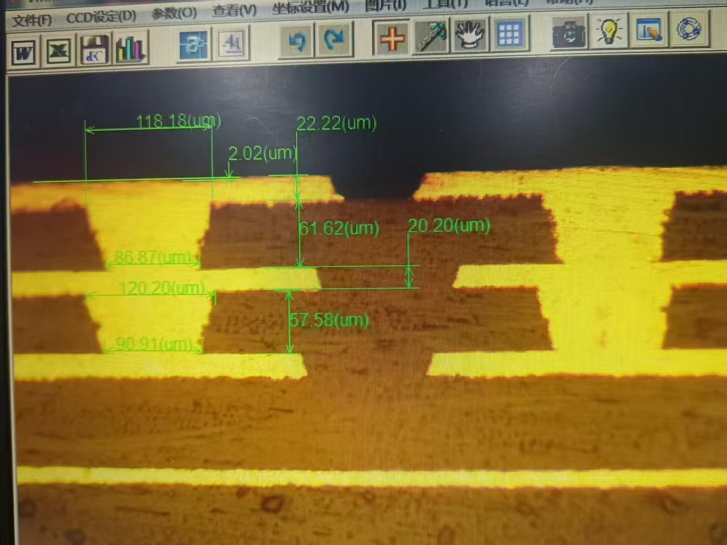
Microvias in the hdi pcb 2 n 2 stackup let you place components closer together. This reduces the size of your board and shortens signal paths. You get better signal integrity because signals travel shorter distances. The sequential lamination process builds each layer carefully, which increases strength and keeps layers aligned. This process improves reliability and performance.
Advantages of 2+n+2 Stackup
You benefit from the 2+n+2 stackup in several ways. The hdi pcb 2 n 2 stackup helps you make devices smaller and lighter. You can add more connections in a compact space, which increases routing density. You maintain strong and clear signals with controlled impedance and reduced signal path lengths. This stackup is ideal for compact devices that need high-density interconnect and excellent signal integrity.
Enables more connections in a smaller area
Maintains high routing density and signal integrity
Supports compact form factors for modern electronics
LT CIRCUIT specializes in manufacturing hdi pcb 2 n 2 stackups. You get advanced any-layer HDI technology, AI-driven quality control, and custom support for your project. LT CIRCUIT helps you achieve the best density, reliability, and signal integrity for your high-density interconnect needs.
Comparing HDI Stackups
1+N+1 vs 2+N+2
When you choose an hdi stackup, you often compare the 1+N+1 and 2+N+2 types. Each offers unique benefits for your printed circuit board design. The 1+N+1 hdi stackup uses a simpler structure. You get two hdi layers that sandwich the core layers. This design works well for moderate complexity and keeps costs low. The 2+N+2 hdi stackup adds more hdi layers on each side. You gain extra routing flexibility and better signal management. This option fits high-performance applications where you need efficient signal paths.
Stackup Type | Description | Application |
|---|---|---|
1+N+1 | Simpler structure with two hdi layers sandwiching N traditional layers. | Balanced performance and cost for moderate applications. |
2+N+2 | More complex with two hdi layers on each side of N traditional layers. | Ideal for high-performance applications requiring efficient signal management. |
LT CIRCUIT offers both 1+N+1 and 2+N+2 hdi printed circuit board solutions. You can use 1+N+1 for MP3 players, GPS units, and simple medical devices. The 2+N+2 stackup works best for smartphones, tablets, and car electronics.
3+N+3 and Other HDI Stackups
If your project needs even more complexity, you can look at 3+N+3 and other advanced hdi stackups. The 3+N+3 hdi stackup gives you the highest routing density and supports the most demanding designs. You often see this type in 5G macro cells, data center transceivers, and automotive systems. The cost and complexity rise with this stackup, but you get unmatched performance.
Stackup Type | Cost | Complexity |
|---|---|---|
3+N+3 | High | High |
1+N+1 | Low | Low |
Other HDI | Varies | Varies |
The 3+N+3 hdi stackup has the highest manufacturing cost.
You need longer lead times because of the complex process.
Simpler hdi stackups like 1+N+1 offer lower costs and faster delivery.
LT CIRCUIT also provides advanced hdi printed circuit board options, including ELIC and any-layer hdi for CPUs, GPUs, and smart car systems. You can match your hdi stackup to your project’s needs, from simple to highly advanced designs.
Choose the Right HDI Stackup
Selecting the best HDI PCB stackup for your project means looking at several important factors. You need to balance design complexity, signal performance, and cost. Each project has unique needs, so you must match the stackup type to your requirements. LT CIRCUIT helps you make these decisions with expert advice and advanced solutions.
Design Complexity
When you design a PCB, the complexity of your stackup affects every step. As you add more layers and use advanced via types, the process becomes more challenging. You see this most in projects with higher component density or when you need to fit many connections in a small space.
HDI PCBs use multiple layers and different vias, which increases design complexity.
The process includes extra steps like drilling and plating, making it more time-consuming.
You can reduce processing time by limiting buried vias and planning your stackup carefully.
As the stackup complexity grows, the number of manufacturing steps increases. This leads to higher manufacturing cost. Careful planning helps you manage both complexity and cost.
For projects with higher component density, you often need stackups like Type III, which use two or more microvia layers. These stackups work best for complex, dense multilayer PCBs. If your design has moderate component density, a simpler stackup like 1+N+1 may be enough.
Signal Performance
Signal integrity requirements play a big role in your stackup choice. High-speed applications need careful attention to signal routing and layer arrangement. If you want improved signal integrity, you must control impedance and minimize signal loss.
High-frequency signals can degrade quickly, causing issues like reflection and crosstalk.
Reduced trace widths and spacing in HDI PCBs can increase the risk of signal degradation.
The right stackup design helps you control impedance and maintain improved signal integrity.
To achieve improved signal integrity, you should:
Optimize trace geometry to reduce signal loss and crosstalk.
Use controlled impedance design to match trace impedance with sources and loads.
Route signals carefully to avoid sharp turns and minimize via usage.
Projects with higher component density and strict signal integrity requirements benefit from advanced stackups like 2+N+2 or 3+N+3. These options support improved signal integrity in high-speed applications, making them ideal for networking, data centers, and advanced consumer electronics.
Cost and Manufacturing
Cost is always a key factor when you choose the right HDI stackup. The number of layers, type of vias, and overall complexity all affect manufacturing cost. As you increase component density or move to higher component density designs, you add more steps to the process.
Maintaining precise registration between layers becomes more difficult as complexity rises.
Uniform plating of deep stacked microvias adds to the manufacturing cost.
Managing thermal stress and achieving high yields require advanced techniques.
You must balance performance needs with cost to avoid overspending.
Here is a simple checklist to help you decide:
Consideration Type | Key Points |
|---|---|
Mechanical | Make sure the stackup meets thickness needs to avoid extra cost. |
Electrical | Plan signal and plane layers to meet signal integrity requirements. |
Fabrication | Define trace width and hole sizes to balance performance and cost. |
Documentation | Provide clear drill charts and component indicators to prevent errors. |
LT CIRCUIT supports you at every step. You get expert advice to choose the right HDI stackup for your project. LT CIRCUIT offers customization options, smart stackup strategies for improved signal integrity, and thorough testing like Flying Probe Test. You can select HDI Any Layer PCBs for higher component density and improved efficiency. This support helps you manage manufacturing cost while meeting your signal integrity requirements and performance goals.
LT CIRCUIT HDI Solutions
Custom HDI PCB Options
You can rely on LT CIRCUIT for a wide range of custom pcb solutions. The company understands that every project has unique requirements. You get support from the first design step to the final pcb product. LT CIRCUIT offers DFM support, which helps you design a pcb that is easy to manufacture. You can test your ideas with prototyping before moving to mass production. The company lets you order any quantity of pcb, whether you need just a few or thousands.
You also receive engineering support to solve design issues early. LT CIRCUIT provides many finishes, such as ENIG or nickel-palladium gold, to match your pcb needs. You can choose materials like Al2O3 or AlN for better heat management in your pcb. The company offers solder mask colors, including black, and you can customize line width or spacing. Your pcb can work in extreme temperatures, from -50°C to 150°C. You get comprehensive support, including troubleshooting and updates, to ensure your pcb fits your project.
Description | |
|---|---|
DFM support | Helps design a board that is easy to build |
Prototyping | Allows testing of designs before mass production |
Order quantity | Flexibility to order few or many boards as needed |
Engineering support | Assistance in resolving design issues early |
Finishes | Options like ENIG or nickel-palladium gold |
Materials | Choices like Al2O3 or AlN for heat management |
Solder mask colors | Options such as black, with customizable line width |
Temperature range | Boards can operate from -50°C to 150°C |
Comprehensive support | Assistance from design to final product |
Design advice | Guidance on design and handling for project fit |
Quality and Innovation
You benefit from LT CIRCUIT’s focus on quality and innovation in every pcb. The company uses advanced testing tools, such as AOI, flying probe tests, X-ray, and thermal testing, to check each pcb. These tools help reduce defects and ensure your pcb meets strict standards. LT CIRCUIT uses laser drilling, digital twin technology, and any-layer HDI processes to create innovative pcb designs. Every pcb goes through rigorous checks to guarantee high quality and reliability.
LT CIRCUIT meets top industry certifications. Your pcb will comply with ISO certifications for quality management and environmental care. The company follows IPC standards, which set strict rules for high-quality pcb production. UL certification ensures your pcb meets electrical safety and fire hazard standards.
You also get strong support services. LT CIRCUIT provides flying probe tests, E-tests, and AOI inspections. The company’s quality assurance system uses advanced equipment to monitor every pcb during production. The accuracy compliance rate for HDI pcb products is over 99.8%. You can trust LT CIRCUIT to deliver reliable, high-performance pcb solutions for your most demanding projects.
You should match your HDI stackup to your project’s needs. The 2+N+2 option offers high routing density, strong signal transmission, and flexibility:
Advantage | Description |
|---|---|
Routing Density | Supports complex, compact designs |
Signal Transmission | Ensures reliable, high-speed performance |
Consider design complexity, cost, and performance. Trust LT CIRCUIT for expert support and proven reliability.
FAQ
What is the main advantage of a 2+N+2 HDI stackup?
You get higher routing density and better signal integrity. This stackup works well for compact, high-performance devices.
How do you choose the right HDI stackup for your project?
You should match your stackup to your design complexity, signal needs, and budget. LT CIRCUIT can help you make the best choice.
Can LT CIRCUIT customize HDI PCBs for special requirements?
Yes! You can request custom materials, finishes, and testing. LT CIRCUIT supports unique designs and offers expert engineering advice.
See Also
Understanding Different Stack-up Configurations for HDI PCBs
Evaluating Costs and Benefits of Advanced HDI PCB Designs
Essential Design Factors for Reliable HDI PCB Production