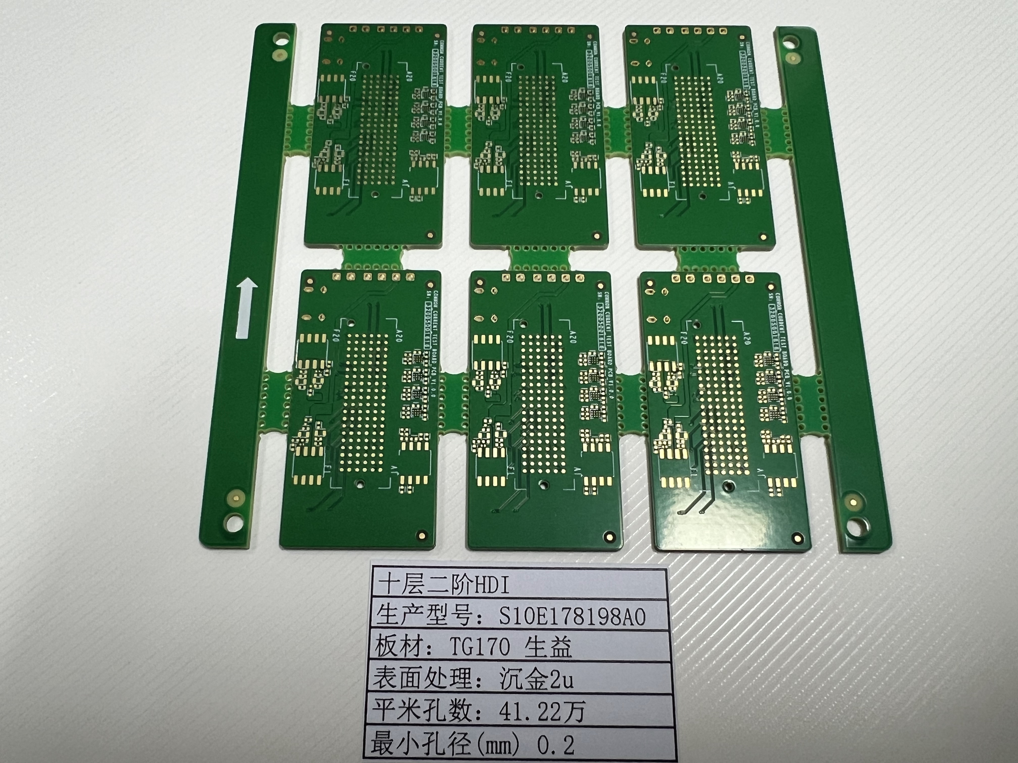
What is 2+N+2 HDI PCB Stackup and How Does Its Structure Work
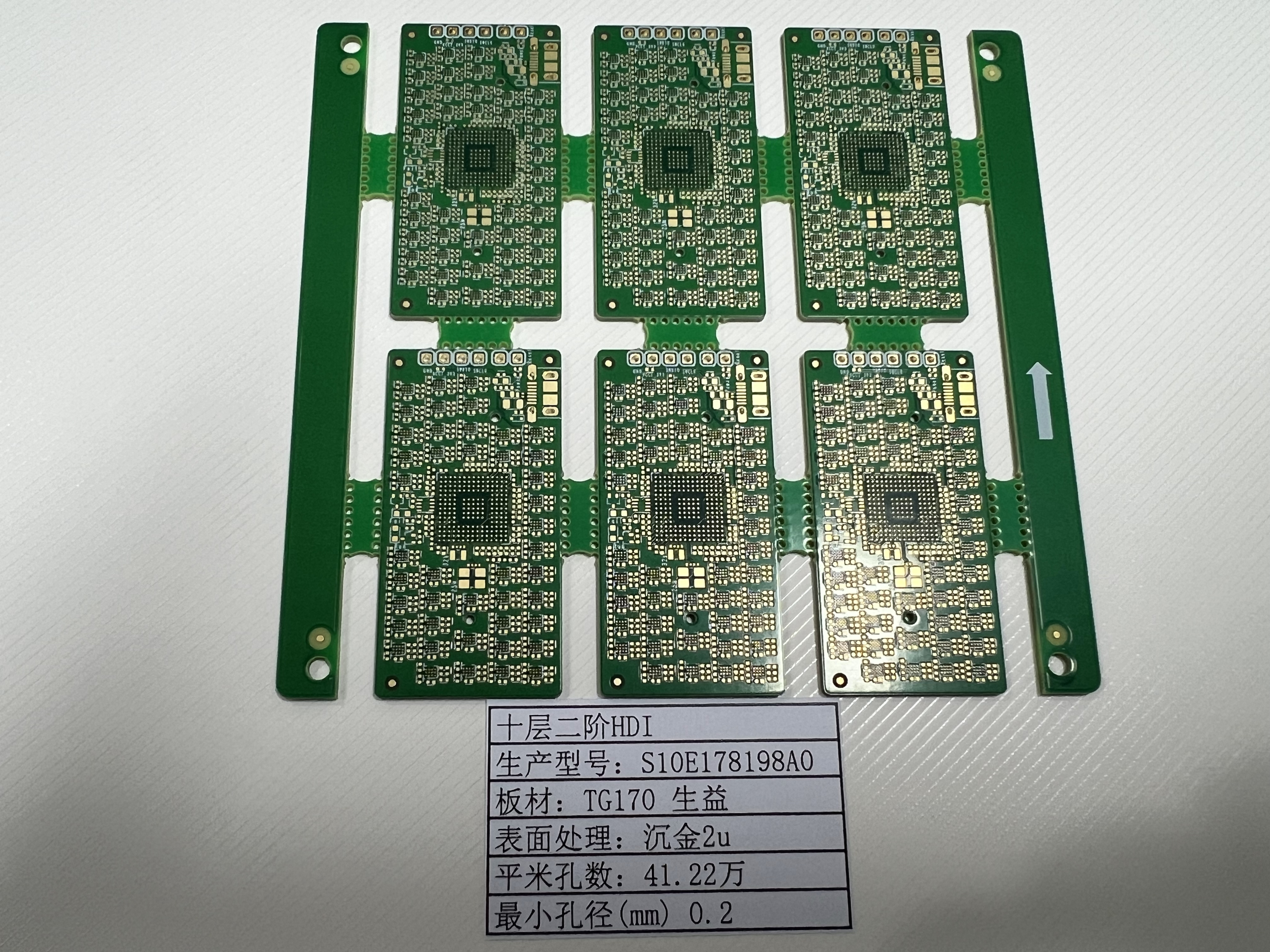
The hdi pcb 2+n+2 stackup refers to a design where there are two HDI layers on each outer side and N core layers in the center. This hdi pcb 2+n+2 configuration is ideal for meeting high-density interconnect requirements in printed circuit boards. The hdi pcb 2+n+2 stackup employs a step-by-step lamination process, resulting in compact and durable PCB designs suited for advanced electronic applications.
Key Takeaways
The 2+N+2 HDI PCB stackup has two layers on the outside. There are N core layers in the middle. Each side also has two buildup layers. This design lets you make more connections. It also helps control signals better.
Microvias connect the layers very closely. This saves space and makes signals better. Sequential lamination builds the stackup one step at a time. This makes it strong and very exact.
This stackup helps make devices smaller, stronger, and faster. Designers should plan early for the best results. They should pick good materials. They also need to use the right microvia methods.
2+N+2 PCB Stackup Structure
HDI PCB 2+N+2 Layer Meaning
The 2+N+2 stackup is a special way to build an hdi pcb stackup. The first "2" means there are two layers on the top and bottom of the pcb. "N" stands for the number of hdi core layers in the middle, and this number can change based on what the design needs. The last "2" shows there are two more layers on each side of the core. This naming system helps people know how many buildup and core layers are in the hdi pcb 2+n+2 configuration.
The two outside layers are where parts go and fast signals travel.
The core layers (N) let designers add more layers, so they can fit more connections and make the board work better.
The buildup layers on both sides help make special via structures and allow for more routing paths.
If you make "N" bigger in the 2+n+2 pcb stackup, you get more inside layers. This lets you put more parts on the board and make more complicated paths. More layers also help keep signals clear, block EMI, and control impedance. But, adding layers makes the stackup harder to build, thicker, and more expensive. Designers have to think about these things to get the best mix of performance and cost in the hdi pcb 2+n+2 structure.
2+N+2 Stack-Up Arrangement
A normal 2+n+2 stackup uses the same number of layers on each side. This keeps the board strong and makes sure it works the same everywhere. The layers are set up to help the board work well.
The top and bottom layers are for signals and parts.
Ground planes are next to signal layers to help signals return and stop interference.
Power planes are in the middle, close to ground planes, to keep voltage steady and lower inductance.
The stackup is kept even to stop bending and keep the thickness the same.
Note: Keeping the stackup even is important. It stops stress and helps the printed circuit board work well.
The materials used in the stackup matter a lot. Common core and buildup materials are FR-4, Rogers, and polyimide. These are picked because they lose little energy and handle heat well. High-end materials like MEGTRON 6 or Isola I-Tera MT40 are used for the hdi core layer. Buildup layers might use Ajinomoto ABF or Isola IS550H. The choice depends on things like dielectric constant, how much energy is lost, heat strength, and if it works with hdi technology.
Core layers often use FR-4, Rogers, MEGTRON 6, or Isola I-Tera MT40 for strength.
Buildup layers can use resin-coated copper (RCC), metalized polyimide, or cast polyimide.
PTFE and FR-4 laminates are also used in hdi pcb stackup designs.
Prepreg is a sticky resin that holds copper layers and cores together. The core makes the board stiff, and prepreg keeps everything stuck and insulated. Using prepreg and core materials in the 2+n+2 stackup keeps the board strong, controls impedance, and keeps signals clear.
Layer Type | Typical Thickness Range | Thickness in Microns (µm) | Copper Thickness |
|---|---|---|---|
Core Layers | 100 to 200 µm | 1 to 2 oz | |
HDI Layers | 2 to 4 mils | 50 to 100 µm | 0.5 to 1 oz |
The stackup design lets you fit lots of connections. Microvias are drilled to link layers close together. This makes the printed circuit boards small and work really well.
Microvias and Lamination
Microvia technology is very important in the 2+n+2 stackup. Microvias are tiny holes made with lasers that connect layers next to each other. There are different kinds of microvias:
Microvia Type | Description | Advantages |
|---|---|---|
Buried Microvias | Connect inside layers, hidden inside the pcb. | Fit more paths, save space, and help signals by making paths shorter and lowering EMI. |
Blind Microvias | Connect the outside layer to one or more inside layers, but not all the way through. | Like buried vias but different in shape and heat handling; they can be affected by outside forces. |
Stacked Microvias | Many microvias stacked on top of each other, filled with copper. | Connect layers that are not next to each other, save space, and are needed for small devices. |
Staggered Microvias | Many microvias placed in a zigzag pattern, not straight up and down. | Lower the chance of layers coming apart and make the board stronger. |
Stacked microvias save space and help make small devices, but they are harder to make. Staggered microvias make the board stronger and less likely to break, so they are good for many uses.
Sequential lamination is the way to build the 2+n+2 stackup. This means making groups of layers, working on them one at a time, and then pressing them together with heat and pressure. Sequential lamination lets you make special vias, like stacked and staggered microvias, and fit lots of connections. It also helps control how layers stick together and how microvias are made, which is very important for hdi pcb stackup designs.
Sequential lamination lets you make microvias as small as 0.1 mm, which helps fit more paths and keeps signals clear.
Doing fewer lamination steps saves money, time, and lowers the chance of problems.
Keeping the stackup even stops the board from bending and getting stressed.
Microvias in the 2+n+2 stackup let you put parts closer together and make the board smaller. Controlled impedance traces and low-loss materials keep signals strong, even at high speeds. Laser drilling can make microvias as small as 50μm, which helps in crowded spots. Putting blind microvias near fast parts makes signal paths shorter and lowers unwanted effects.
The 2+n+2 stackup, with its special microvia and lamination methods, lets designers make small, strong, and high-performing printed circuit boards. This is needed for modern hdi technology and works for many different uses.
2+N+2 Stackup Benefits and Applications
HDI PCB Stackup Advantages
The 2+n+2 stackup has many good points for today’s electronics. This setup helps make devices smaller and lets more connections fit in a small space. It also keeps signals strong and clear. Microvias and special via-in-pad tricks let designers add more paths without using up much room. This is important for fast and tiny gadgets. The table below shows the main benefits:
Benefit | Explanation |
|---|---|
Improved Reliability | Microvias are shorter and stronger than old-style vias. |
Enhanced Signal Integrity | |
Higher Density | Microvias and extra layers let more connections fit in. |
Smaller Size | Blind and buried vias save space, so boards can be smaller. |
Cost-effectiveness | Fewer layers and smaller boards mean lower costs. |
Better Thermal Performance | Copper foil spreads heat well, which helps with power. |
Mechanical Strength | Layers of epoxy make the board tough and hard to break. |
HDI PCB stackup designs help make smaller, stronger, and cheaper products for fast electronics.
2+N+2 Stackup Use Cases
The 2+n+2 stackup is used in many fields that need lots of connections and fast data. Some common uses are:
Phones and tablets for everyday use
Car electronics for smart driving
Machines that control factories
Medical tools that need small, strong boards
Tools for testing and measuring things
These areas use the 2+n+2 stackup because it fits many connections in a small space and works well.
Design and Manufacturing Tips
Designers should follow some simple steps to make sure 2+n+2 stackup PCBs work well:
Use stacked or staggered microvias that are not too tall.
Pick core and prepreg materials that keep signals steady and handle heat.
Put fast signal layers close to ground planes for better signals.
Use thin lines and small pads for traces and vias.
Do not use sharp angles in traces to avoid problems.
Work with skilled HDI makers to match design and building steps.
Picking the right materials and making vias carefully keeps signals steady and helps 2+n+2 stackups work fast.
The 2+N+2 HDI PCB stackup has two signal layers on the outside. It also has N core layers in the middle. This stackup is made using a step-by-step lamination process. Microvias are used to connect the layers and fit lots of paths. Engineers like this stackup because it works well and is not too hard to make. It is a good choice for BGA designs with many pins. It also works for small boards that need strong connections.
FAQ
What does "2+N+2" mean in HDI PCB stackup?
"2+N+2" means there are two buildup layers on each side. There are also N core layers in the middle. This setup lets the board handle lots of connections. It also helps signals stay strong and clear.
Why do engineers use microvias in 2+N+2 stackups?
Microvias link layers that are next to each other. They help save space on the board. They also make signals better and let the board be smaller and more reliable.
Microvia Type | Benefit |
|---|---|
Blind | Saves space |
Buried | Shorter signals |
Can 2+N+2 stackups support high-speed signals?
Yes. This stackup uses special materials that keep signals steady. Engineers can send fast signals without losing quality in new devices.
See Also
Understanding Common Stack-Up Configurations In HDI Multilayer PCBs
Evaluating Costs And Benefits Of Advanced HDI Microvia Designs
The Process Behind Designing And Producing HDI Any Layer PCBs
Essential Design Factors For Reliable HDI High-Density Interconnect PCBs