What is Back Drilling in HDI PCB Manufacturing?
Back drilling in HDI PCB manufacturing involves the removal of extra via parts, which helps maintain signal clarity by preventing distortions and echoes. This process of HDI PCB back drill reduces crosstalk and enhances the performance of high-speed circuits. LT CIRCUIT excels in providing back drill solutions, ensuring accuracy and reliability for advanced applications.
Key Takeaways
Back drilling takes out extra via stubs in HDI PCBs. This helps signals stay clear and reduces noise in fast circuits.
It makes the PCB work better by cutting down EMI and keeping signals strong in multilayer boards.
Accurate back drilling is very important. Using good tools and methods makes clean cuts and keeps PCB layers safe.
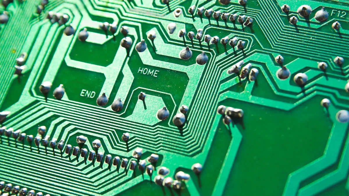
Understanding HDI PCB Back Drill
What is Backdrilling in HDI PCBs?
Backdrilling is a way to remove unused parts of vias. These unused parts, called stubs, can mess up signals in fast circuits. Stubs reflect signals and cause interference, making circuits less clear. Backdrilling cuts off the stubs, helping signals move smoothly and reducing noise. This is very useful for HDI PCBs, which need careful signal control because of their dense design.
The process focuses on specific vias that link PCB layers. By drilling from the back of the board, extra via sections are removed, leaving only the needed part. This helps stop signal reflections and keeps impedance steady. Both are important for fast communication systems and sensitive circuits.
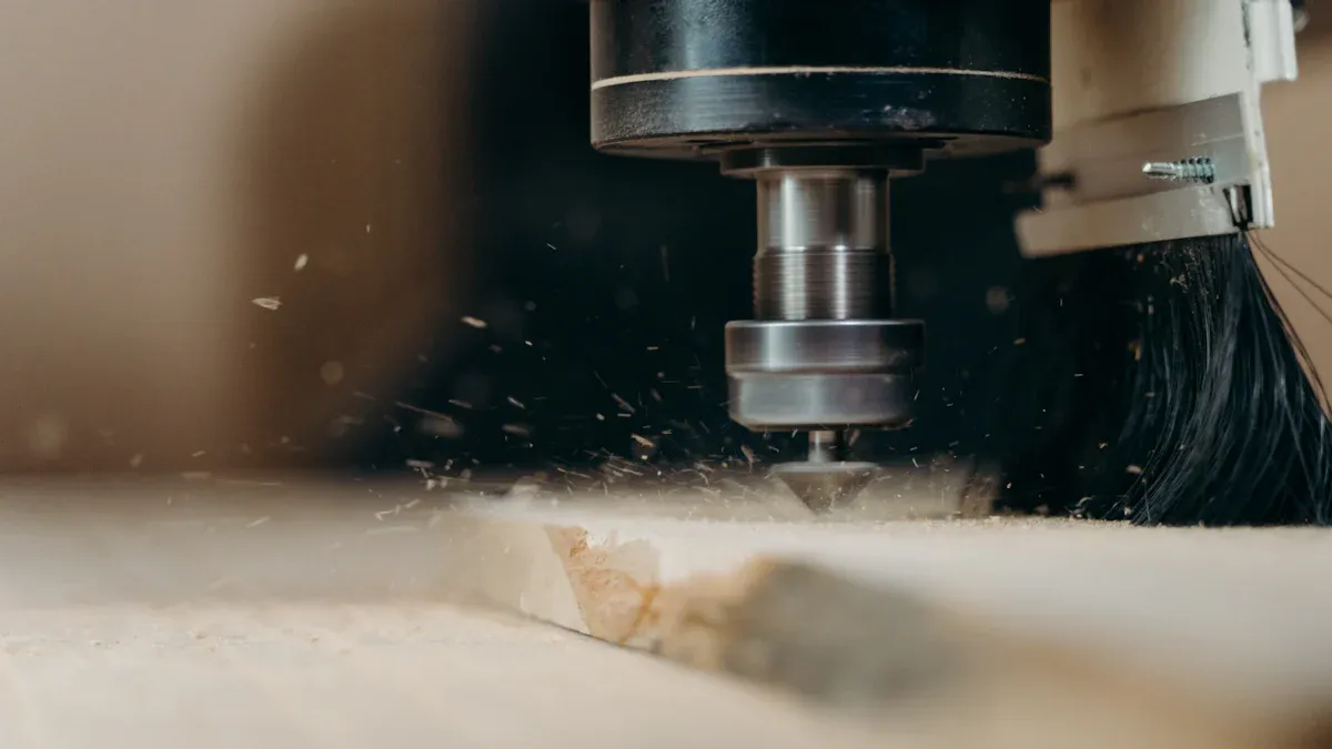
How Does the Backdrill Process Work?
First, engineers find vias that need fixing. They check the PCB design to spot stubs that might harm signals. Then, a special drill removes the extra via part, making a clean back drill hole. This step needs to be precise to avoid damaging the PCB's working layers.
The machines used for backdrilling must be very accurate. Advanced tools ensure the cut is clean and doesn’t harm nearby materials. This accuracy keeps the PCB strong and ensures it works well in fast systems.
The Role of Stub Length in Signal Quality
The length of a stub affects how good a signal is. A stub can act like a tiny circuit, storing energy at certain frequencies. If a signal matches this frequency, it can weaken and lose clarity. This can also cause timing problems, called jitter.
When a signal moves through a via, it splits where the stub starts. The stub acts like a dead-end path, bouncing signals back. These bounces can mess up the original signal, causing errors and interference. Shortening the stub with backdrilling fixes this and improves the PCB’s performance.
Backdrilling is a trusted way to solve signal problems in fast designs. It makes signals clearer, reduces interference, and is key in modern PCB manufacturing.
Benefits of PCB Back Drilling
Improved Signal Integrity in High-Speed Designs
Backdrilling helps improve signal quality in fast circuits. Via stubs can reflect signals and cause interference. Removing these stubs allows signals to travel smoothly. This process also reduces jitter, making communication systems more reliable.
Tests show that fewer chips stick to the drill bit as feed rate increases. However, the hole plugging rate rises with higher feed rates. Faster spindle speeds help remove chips better and reduce drilling force.
This research solves hole plugging issues in backdrilling. It supports high-speed signal flow and reduces product waste, which is important for advancing backdrilling technology.
Using backdrilling improves signal clarity and reduces disruptions in fast designs.
Reduced Electromagnetic Interference (EMI)
Electromagnetic interference (EMI) can harm electronic devices, especially in high-frequency systems. Backdrilling removes via stubs that act like tiny antennas, reducing EMI. These stubs can send out unwanted waves that interfere with nearby parts.
A telecom company used backdrilling in 5G hardware. This cut EMI by 40% and supported frequencies up to 28 GHz.
Backdrilling ensures cleaner signals and better electromagnetic compatibility (EMC) in your designs.
Enhanced Performance in Multilayer PCBs
Multilayer PCBs are common in modern electronics but can have signal issues. Backdrilling fixes these problems by removing stubs. This reduces reflections, improves impedance, and lowers crosstalk. These changes boost system performance.
Improvement Description | |
|---|---|
Signal Integrity | Better by cutting down reflections and ringing |
Insertion Loss | Lowered, improving signal quality |
Impedance Matching | Enhanced for stronger connections |
Crosstalk Between Vias | Reduced, improving overall function |
Data Rates | Higher speeds possible without stubs |
Channel Bandwidth | Wider, allowing more data to pass through |
System Performance | Improved across all metrics |
EMI Reduction | Less radiation from stub-related issues |
EMC Improvement | Better resistance to outside interference |
Backdrilling unlocks the full potential of multilayer PCBs. It ensures they work reliably and perform at their best.
Factors That Affect Backdrilling Success
PCB Material and Thickness
The type and thickness of the PCB matter for backdrilling. Different materials behave differently when drilled. Strong materials and good heat conductors make drilling easier. Fragile materials, like some fiberglass, can crack under pressure. Thick copper layers wear out drill bits faster, lowering performance.
High Tg materials need special care because they don’t handle heat well. Controlled drilling depth prevents overheating and keeps cuts clean. Engineers use thrust force models to match drilling settings with material properties for the best results.
Evidence Description | Key Points |
|---|---|
Thrust Force Model | Shows how material and drilling settings affect quality. |
Strong materials and heat conductors improve drilling.
Fragile materials need extra care to avoid cracking.
Thick copper layers wear out drill bits faster.
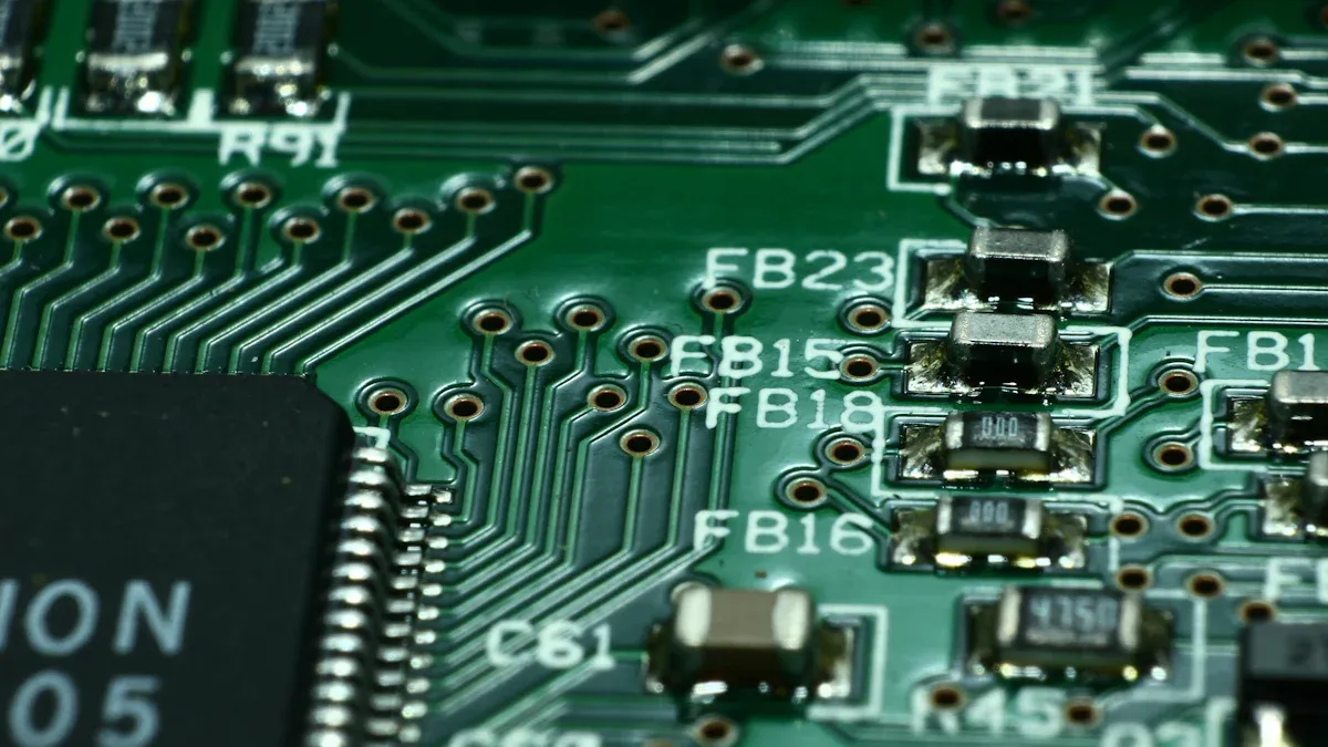
Via Size and Design Details
The size and design of vias affect backdrilling results. Small vias need careful drilling to avoid damaging nearby layers. Big vias are easier to drill but may leave longer stubs. Long stubs can mess up signals, so vias should be placed carefully.
Controlled depth drilling removes only the unneeded stub parts. This keeps the PCB layers safe and improves signal flow. Good via designs reduce problems like jitter and interference, making circuits work better.
Precision and Equipment at LT CIRCUIT
Good tools and precise methods are key for backdrilling. LT CIRCUIT uses advanced machines to make accurate holes and place components correctly. Automated checks find mistakes quickly, keeping quality high.
Quality Control Metric | Description |
|---|---|
Advanced Machines | Use modern tools for accurate drilling and placement. |
Real-Time Monitoring | Detects problems during production to maintain quality. |
Testing Methods | Ensures products meet high standards through thorough testing. |
Engineers check files before production starts.
Quality control monitors production steps closely.
Tests ensure products are strong and reliable.
LT CIRCUIT’s focus on quality ensures your PCBs are made with care. Their backdrilling expertise improves performance for fast designs.
Back drilling is important in PCB making. It removes extra via stubs, making signals clearer and reducing jitter in fast circuits. Tools like CNC and laser drills help ensure accuracy. LT CIRCUIT uses advanced techniques and strict checks. This makes them a reliable choice for better HDI PCB performance and strength.
FAQ
What does back drilling do in HDI PCBs?
Back drilling takes out extra via stubs. This makes signals clearer, lowers interference, and helps fast circuits work better in modern PCB designs.
Can back drilling harm PCB layers?
No, back drilling uses careful tools to protect working layers. The right machines and methods make it safe and effective.
Why pick LT CIRCUIT for back drilling?
LT CIRCUIT uses top tools, live monitoring, and strict checks. This ensures strong, high-quality HDI PCBs made just for you.
See Also
Achieving A Smoother Finish In HDI PCB Laser Drilling
Advantages Of LDI Exposure Machines For HDI PCB Circuits
Explore Cutting-Edge Techniques For HDI PCB Prototyping
Understanding The Design And Production Of HDI Any Layer PCBs
Utilizing Horizontal Copper Sinking Technology In PCB Manufacturing