Understanding HDI PCB Definition and How They Are Made
The hdi pcb definition refers to the foundation for compact and advanced electronics. HDI PCB features thinner lines, smaller vias, and accommodates more components within limited space. Nearly half of modern devices utilize HDI PCB, highlighting a significant shift in the industry. LT CIRCUIT stands out as a leading provider of innovative HDI PCB solutions for today’s technology.
Key Takeaways
HDI PCBs have small holes and thin lines. This lets them hold more parts on smaller, lighter boards. Devices can be faster and smaller because of this.
Special steps like using lasers to drill and stacking layers are used. These steps make HDI PCBs strong and dependable. They work well in today’s electronics.
Picking HDI PCBs makes devices work better and saves space. It also helps new things like 5G, medical tools, and smart wearables.
HDI PCB Definition
What Is HDI PCB?
You might ask what the hdi pcb definition is and why it is important. HDI means high density interconnect. This is a kind of printed circuit board that fits more wiring, pads, and parts into a small space. The hdi pcb definition gives you a printed circuit board with thinner lines, smaller holes, and more connections. These things help you make smaller, lighter, and stronger electronic devices.
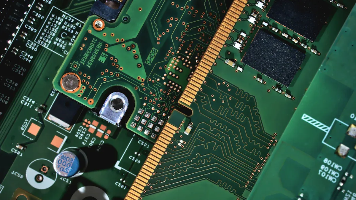
Industry rules say hdi pcb are printed circuit boards with lots of wiring in each area. You will see things like microvias, blind vias, and buried vias. These tiny holes link different layers of the board. HDI boards use special build-up lamination and give high signal performance. You often find hdi pcb in phones, tablets, and other small devices because they save space and work better.
The hdi pcb definition also talks about special layer setups. For example, you might see a (1+N+1) or (2+N+2) stack-up. These show how many layers have microvias and how many are normal. Microvias in hdi pcb are usually less than 0.006 inches wide. This small size lets you fit more connections in less space.
Key Features
When you look at a high-density interconnect pcb, you will see some main features that make it different from regular printed circuit boards. Here are the main things:
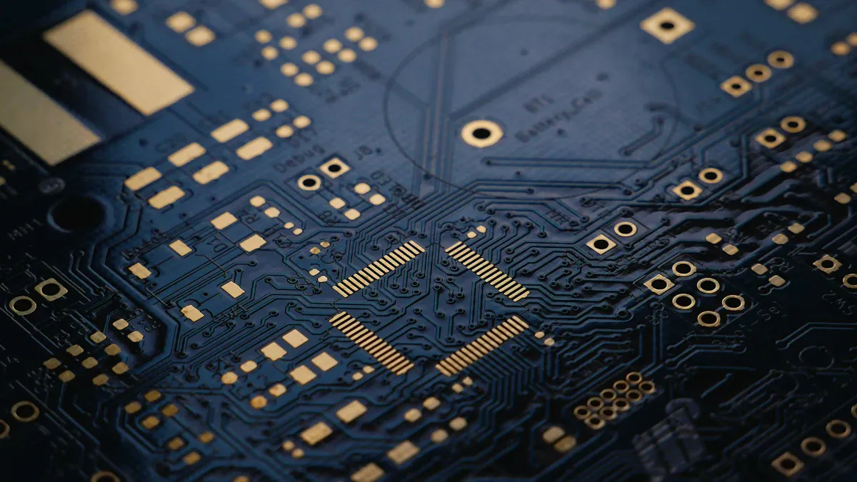
Microvias, Blind Vias, and Buried Vias: These tiny holes link layers but do not use much space. Microvias are smaller than 150 micrometers. Blind vias link the outside layer to an inside layer. Buried vias link two inside layers.
Finer Lines and Spaces: HDI pcb uses lines and spaces as small as 0.1 mm. This lets you make more complex circuits in a small area.
High Pad Density: You can fit over 50 pads in one square centimeter. This means you can put more parts on both sides of the board.
Advanced Manufacturing: HDI pcb uses laser drilling and build-up lamination. These ways make exact features and strong links.
Superior Electrical Performance: Shorter signal paths and better signal quality help your devices work faster and better.
Compact Size and Light Weight: The hdi pcb definition means you get smaller, thinner, and lighter boards. This is great for portable and wearable electronics.
Tip: HDI pcb works with high pin count and small pitch parts. This makes it perfect for advanced electronics like smartphones and medical devices.
Feature | HDI PCB | Standard PCB |
|---|---|---|
Via Technology | Microvias, blind and buried vias | Through-hole vias |
Wiring Density | High, with finer traces and smaller pads | Lower, with larger traces and pads |
Size and Weight | Smaller and lighter | Larger and heavier |
Electrical Performance | Superior, supports high-speed signals | Adequate for low-frequency signals |
Manufacturing Techniques | Laser drilling, via-in-pad, lamination | Mechanical drilling |
Component Compatibility | High pin count, small pitch | Limited for high pin count |
You will see that the hdi pcb definition is about getting the most density and best performance. These things make high-density interconnect pcb the best pick for modern electronics. When you pick hdi pcb, you get a printed circuit board that fits today’s technology needs.
Importance
Why Use HDI PCB?
HDI PCB is used in many new electronics. It has many benefits over regular boards. Companies pick HDI for different reasons:
You get better signal quality with microvias and controlled impedance.
HDI PCB helps heat move away, so devices stay cool.
Small design lets you put parts close together. This saves space and makes things lighter.
HDI boards can bend to fit curved shapes. This gives more ways to design devices.
These boards last longer, even in tough places, without extra layers.
You can fit more parts in a small area. Copper pillars and new methods help with this.
Electricity moves better, so signals stay strong and clear.
HDI PCB blocks electromagnetic noise. This helps devices work well.
New ways to make HDI PCB mean faster building and more layers.
Surface resistance stays low. This is good for high-speed signals.
LT CIRCUIT is a top company for HDI PCB. They make strong boards with careful testing and strict rules. Their flying probe tests and checks make sure every board is high quality.
Industry Applications
HDI PCB is used in many electronics. You see these boards in cameras, laptops, scanners, and phones. HDI makes devices smaller, lighter, and stronger.
Industry | Types of Products / Applications |
|---|---|
Automotive | Navigation systems, GPS, consoles |
Consumer Electronics | Smartphones, laptops, computers, digital cameras, wearable electronics |
Industrial Equipment | Control units, signal modules |
Telecommunications | 5G/6G network equipment |
Medical Devices | Medical electronic devices |
Aerospace & Avionics | Avionics systems |
Military Applications | Military-grade electronic systems |
LT CIRCUIT helps these industries by making HDI PCB with high density and strength. Their skills in laser drilling, EMI modeling, and heat control give you great results. You can count on LT CIRCUIT for HDI PCB in tough jobs, from phones to medical tools.
Benefits
Space and Weight
When you use hdi pcb, you save space and weight. HDI boards let you put more circuits in a small spot. This is because of things like microvias and blind vias. These features help you use thinner and lighter materials. Your device gets lighter and smaller but still works well. You do not lose any important functions. Many phones and tablets use hdi pcb to stay thin and easy to carry.
HDI pcb lets you fit more wires in less space.
Devices get lighter with thin materials.
Special connections help you save room inside.
You can make small products that still work great.
Tip: If you want very thin electronics, hdi pcb is the best way to save space and weight.
Performance
HDI pcb helps your device work better in many ways. You can add more parts in a small area. This makes your device faster and smarter. Small traces and vias help signals move quickly. Shorter paths mean better signals and less noise. HDI pcb also makes your device more reliable. The tight design helps heat move away and stops problems. You can use hdi pcb for things like 5G, IoT, and AI. These need high density and strong boards.
Small size lets you add more cool features.
Better electrical work means less signal loss.
Clearer signals come from strong signal paths.
HDI pcb works for hard designs in new tech.
Strong microvias and layers make boards last longer.
Note: HDI pcb helps you get better performance and strong boards for tough jobs.
HDI PCB Manufacturing Process
Making an hdi pcb takes many careful steps. Each step must be done right to make a good board. LT CIRCUIT uses new ways and strict checks to make sure their hdi pcb is the best. Let’s see how hdi pcb are made.
Design and Materials
First, you design the board. You pick how many layers you need. You also choose what materials to use. Most hdi pcb use FR4 because it is strong and does not burn easily. For fast or special devices, you might use polyimide, BT-epoxy, or PTFE. These help stop signal loss and keep the board steady. Copper is used for the circuits because it carries electricity well. The solder mask is made from special materials that protect the board.
Tip: Picking the right material helps your hdi pcb handle heat and work fast.
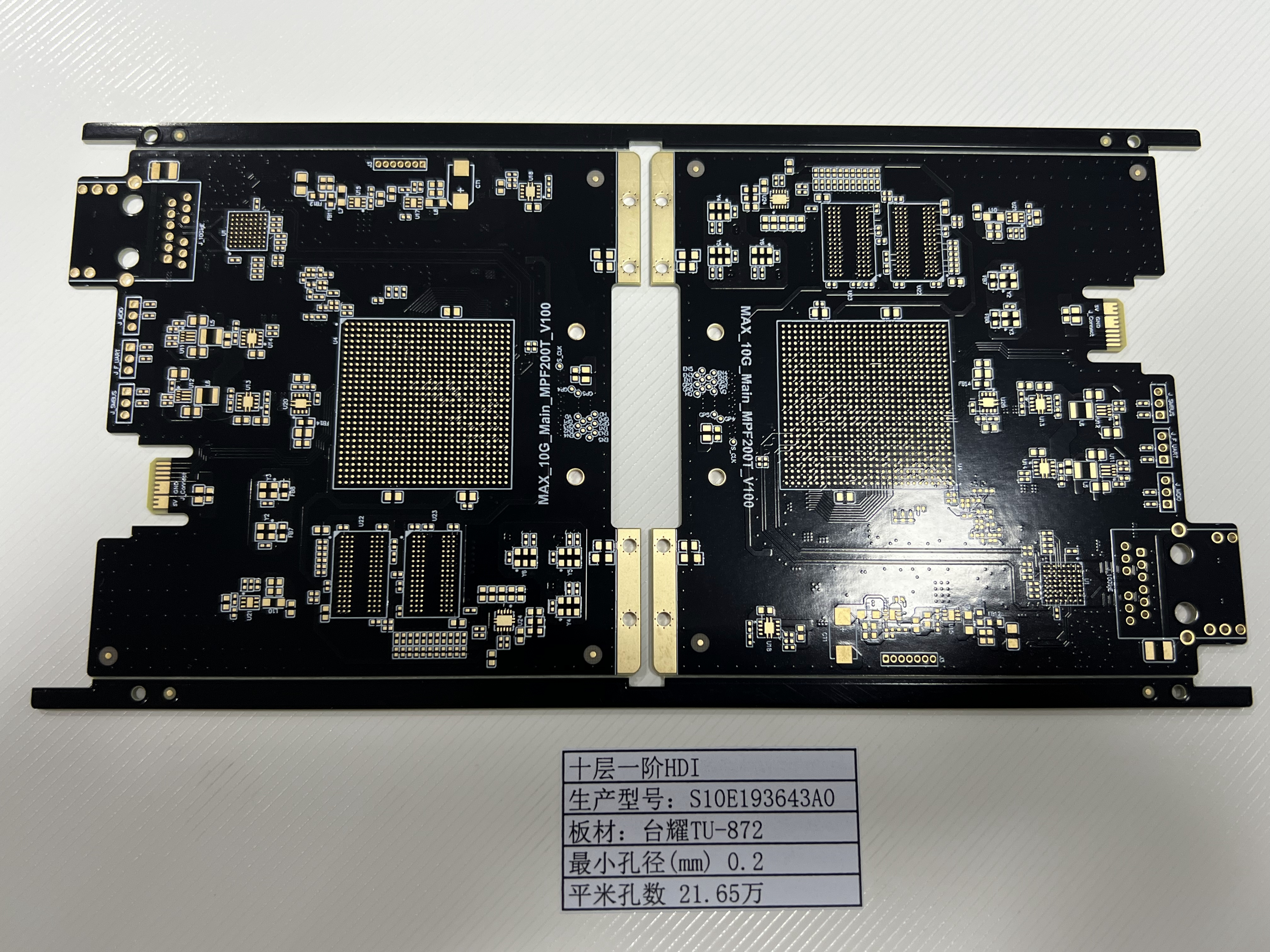
Layer Stackup
Next, you set up the layers. You put them in an order that fits your circuit. A normal hdi pcb has signal, power, and ground layers. Microvias, blind vias, and buried vias connect these layers. LT CIRCUIT makes sure each layer is in the right place. How you stack the layers changes how well your board works.
Layer Type | Function |
|---|---|
Signal Layer | Carries data and power |
Power Layer | Sends out voltage |
Ground Layer | Cuts down noise |
A good stack of layers helps your hdi pcb work better and last longer.
Microvia Drilling
Drilling microvias is very important. You use lasers to make tiny holes called microvias. These holes are much smaller than normal ones. Microvias link one layer to another but do not take up much space. LT CIRCUIT uses special laser machines for this job. Microvias let you fit more circuits in a small spot. This step also helps signals move faster and better.
Note: Microvias make your hdi pcb smaller, lighter, and good for fast signals.
Lamination Process
Lamination means pressing all the layers together. You use heat and pressure to make one solid board. For hdi pcb, you often use sequential lamination. This means you add layers and drill microvias in steps. LT CIRCUIT uses this way to make boards with many layers. You can make stacked microvias and tricky designs.
Heat and pressure stick the layers together.
Drill and plate microvias after each step.
Repeat for more layers.
This makes your hdi pcb strong and reliable.
Plating and Filling
After lamination, you plate and fill the microvias. You cover the microvias with copper so they carry electricity. LT CIRCUIT uses special plating lines for even copper. Sometimes, you fill the microvias with copper to make the surface flat. This is needed when parts sit right on top of the vias. Good plating and filling help your board work better and last longer.
Technique | Purpose |
|---|---|
Makes a thin copper layer in the holes | |
Electroplating Filling | Fills microvias for flat, strong links |
Doing plating and filling right helps your hdi pcb stay strong.
Surface Finish
The surface finish keeps the copper safe and helps with soldering. For hdi pcb, you want a flat and smooth finish. ENIG is a top choice. It gives a flat surface, stops rust, and works with tiny parts. Immersion tin is another good finish for hdi pcb. LT CIRCUIT offers different finishes for your needs.
Surface Finish | Key Properties | Best Use for HDI PCB |
|---|---|---|
ENIG | Flat, stops rust, very reliable | Tiny parts, high quality |
Immersion Tin | Flat, no lead, easy to solder | Tiny parts, RoHS safe |
HASL | Not flat, not good for tiny parts | Not best for hdi pcb |
A good finish helps you put parts on the board and keeps it working well.
Testing and Inspection
Testing and checking are very important. You check every board to make sure it is good. LT CIRCUIT uses machines to look for problems. They use AOI, X-ray, and flying probe testers. These tools find bad microvias, wrong layers, or broken lines. You also test for shorts and open spots. For boards that must last, you test with heat and cold. These steps make sure your hdi pcb works in real life.
Tip: Careful testing and checking help you avoid problems and keep your devices safe.
Assembly
The last step is assembly. You put and solder parts onto the board. HDI assembly uses tiny parts and needs careful work. You may use machines for very small parts. LT CIRCUIT can handle boards with many layers and microvias. You must control heat and stress to keep the board safe. Careful assembly makes sure your hdi pcb works right.
Place tiny parts very carefully.
Solder with just the right heat.
Check finished boards for quality.
Assembly is the last step before your hdi pcb is ready to use.
Note: LT CIRCUIT’s careful work and checks give you hdi pcb you can trust.
Key Techniques
Laser Drilling
Laser drilling is a very important way to make hdi pcb. This process makes tiny holes called microvias. These holes can be as small as 0.075 mm. Mechanical drilling cannot make holes this small. Laser drilling does not touch the board, so the drill does not wear out. You do not have to worry about dirt from the drill. The laser makes smooth hole walls. This helps copper stick better when plating. The laser burns away material and leaves less mess. Laser drilling puts holes in the right spot, even within ±0.01 mm. This accuracy lets you add more connections in a small space. Your pcb becomes smaller and works better.
Laser drilling makes very tiny microvias.
This process lets you fit more wires and keeps signals strong.
Your pcb lasts longer and works well.
Sequential Lamination
Sequential lamination is another important way to make hdi pcb. You build your pcb by adding layers one at a time. Each layer is bonded before adding the next. This method works with blind and buried vias. You can use smaller vias and make more complex boards. Some pcb can have up to 20 layers. Sequential lamination helps keep signals clear by controlling impedance. This is good for fast circuits. The process also stops the board from bending too much. You need special machines and skilled workers for this. It can take longer to finish, but it helps with tricky designs.
Tip: Sequential lamination lets you design more types of boards and fit more parts.
Fine Line Etching
Fine line etching is a key step in making hdi pcb. This process makes very thin lines and small spaces. Sometimes, lines are only 0.05 mm wide. You can fit more circuits in a tiny area. Fine line etching uses special photoresist and chemicals to keep lines exact. This helps make small pcb for things like smartphones. Fine line etching lets you add more wires without hurting signal quality or making the board hard to build.
Fine line etching lets you fit more wires in less space.
This process helps you make smaller and stronger devices.
Challenges
Manufacturing Complexity
Making HDI pcb is much harder than making standard pcb. Standard pcb use simple holes and easy steps. HDI pcb need special ways like laser drilling for microvias. They also use sequential lamination and careful imaging. You need skilled workers and special machines for these jobs. The design is tricky because you must fit tiny features and more layers in a small space. This makes building the board take longer and cost more money. It is harder to make many HDI pcb at once than standard boards. Every step must be checked to make sure the board works well.
HDI pcb need laser drilling and special lamination.
You must use careful imaging for tiny lines.
Skilled people and advanced machines are needed.
More complex designs mean more time and higher cost.
PCB Type | Manufacturing Complexity | Cost | Reliability |
|---|---|---|---|
Standard PCB | Low | Lower | Good |
HDI PCB | High | Higher | Excellent |
Quality Control
Quality control is very important for HDI pcb. You must watch out for problems like crosstalk, noise, and impedance issues. These can cause mistakes and make devices fail. Good routing, ground planes, and strict rules help stop these problems. Testing helps you find mistakes early. You must check for shorts, open spots, and things like heat and wetness. Some common problems are broken circuits, bad soldering, weak materials, and poor process control. You can fix these by making better designs, checking materials, and using good testing tools. Training your team and having strong quality rules help keep boards reliable.
Tip: Watching the process all the time helps you find problems before they get worse.
Scratches and copper showing need careful handling.
Bending and warping come from bad materials or steps.
Bad impedance control hurts RF work.
Soldering problems need strict testing and good steps.
You must pay attention to every step to keep HDI pcb strong and ready for tough jobs.
Future Trends
Technology Advances
Many new changes are coming for HDI PCB technology. AI design tools help you make boards faster. They also help you make fewer mistakes. Miniaturization lets you add more features in small spaces. This helps IoT, 5G, and medical devices grow. Advanced inspection methods like AOI and X-ray checks find tiny problems. These methods help improve board quality.
AI makes design quicker and checks for errors.
Miniaturization puts more functions in small devices.
AOI and X-ray checks find problems early.
HDI PCBs now work with fast data and better power use.
New materials help boards handle heat and keep signals strong.
You can put parts inside the board to save space.
LT CIRCUIT uses laser drilling and digital twin technology. They also use any-layer HDI processes. Their factories have clean rooms and fast plating lines. This means you get good boards quickly. They use eco-friendly materials and smart design rules. These things help lower costs.
Industry Outlook
The HDI PCB market will keep growing. People want smaller, faster, and stronger electronics. Experts think the market will grow a lot in the next ten years. This is because of 5G, IoT, and electric cars. Asia Pacific will stay the main place for making boards.
Aspect | Details |
|---|---|
Projected CAGR (2025-2033) | About 8% |
Market Size 2025 | $15 billion |
Market Size 2033 | $28 billion |
Key Growth Drivers | Miniaturization, 5G, IoT, automotive, HPC |
Regional Outlook | Asia Pacific leads |
Challenges | High cost, design complexity |
LT CIRCUIT gets ready for these changes. They offer fast prototyping and flexible help. They follow strict quality rules. You can trust them to make advanced HDI PCBs for telecom, aerospace, and medical needs.
You can see that HDI PCBs help make today’s electronics better.
Good design and special materials like FR4 or polyimide help signals stay strong.
Using lasers to drill and careful lamination make the boards last longer.
LT CIRCUIT checks every board closely and uses new tools for great results.
Key Takeaway | Explanation |
|---|---|
New ideas make devices better | LT CIRCUIT’s smart ways help lead the industry. |
Keep looking for new HDI PCB ideas in the future!
FAQ
What makes HDI PCBs different from standard PCBs?
HDI PCBs have smaller holes and thinner lines. They also hold more parts than standard PCBs. These things let you make smaller and faster devices.
Can you use HDI PCBs in medical devices?
Yes, HDI PCBs work in medical devices. They help make equipment that is small, strong, and works well for healthcare.
How does LT CIRCUIT ensure HDI PCB quality?
LT CIRCUIT checks every board with special testing tools. They use AOI and flying probe tests to look for problems. This helps make sure you get good boards every time.
See Also
Step-By-Step Process For Designing And Manufacturing HDI PCBs
Explore Cutting-Edge Methods For HDI PCB Prototyping Now
Essential Design Tips For Producing Reliable High-Density HDI PCBs
Advantages Of Employing LDI Exposure Machines In HDI PCB Production
Understanding The Process Behind Laser Hole Via Filling In HDI PCBs