High-Frequency HDI PCB Design: Material Selection and Stackup Strategies for Optimal Signal Performance
Engineers notice quick changes in signal performance when they pick the right materials and stackup in HDI PCB Design. Using advanced materials and making careful stackup choices help keep signal integrity at high frequencies. LT CIRCUIT gives useful solutions, using strong knowledge and new ideas in high-frequency PCB manufacturing.
Key Takeaways
Picking materials with low dielectric constants and low loss factors helps high-frequency signals stay fast and clear. This reduces signal loss and distortion.
Good stackup designs with the right layer setup and strong reference planes make signal integrity better. They also cut down on electromagnetic interference and help lower manufacturing costs.
Making vias and trace routing better by using microvias and keeping the right spacing stops signal reflections and crosstalk. This makes sure high-speed PCB performance stays reliable.
Material Impact
Dielectric Properties
Dielectric properties are very important for high-frequency PCB performance. Engineers pick materials with certain dielectric constants (Dk) and dissipation factors (Df). This helps control how fast signals move and keeps signal loss low. If a material has a lower Dk, signals move faster and there are fewer delays. A lower Df means less signal loss, so signals stay clear at high frequencies.
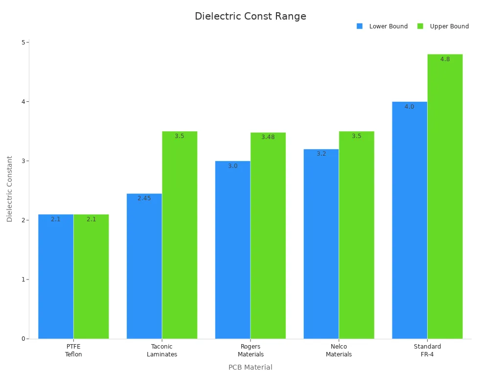
Tip: Picking materials with a dielectric constant from 2.1 to 3.5 is best for high-frequency use. These materials let signals move faster and help stop signal loss.
The table below shows some common PCB materials and their dielectric constant ranges:
PCB Material | Dielectric Constant Range (Dk) | Notes on High-Frequency Suitability |
|---|---|---|
PTFE (Teflon) | ~2.1 | Preferred for minimum signal loss and high speed |
Taconic Laminates | 2.45 to 3.5 | Suitable for RF and microwave applications |
Rogers Materials | 3.0 to 3.48 | High-performance laminates for high-frequency circuits |
Nelco Materials | 3.2 to 3.5 | Used in high-frequency PCB applications |
Standard FR-4 | 4.0 to 4.8 | Generally less suitable for very high-frequency but common |
Research shows some important things about dielectric properties and signal performance:
Dielectric constant (Dk) and loss tangent (Df) both change high-frequency signal quality.
Using low Dk laminates lets you make thinner boards or wider traces, which can lower losses.
Making traces wider only helps a little with signal loss, but low Df laminates help much more.
The loss properties (Df) of a material matter more for signal integrity than just changing Dk for wider traces.
Low-Loss Materials
Low-loss materials are needed to keep signals strong in high-frequency uses. These materials, like PTFE and ceramic-filled epoxy, have low dielectric constants and low dissipation factors. They help stop signal weakening and distortion, so signals stay strong and clear even at high speeds.
Tests show that low-loss materials help signals travel better by cutting down on reflection and noise. Engineers use special tests like S-parameter measurements, eye diagrams, and time-domain reflectometry to check these benefits. For example, S-parameters show that low-loss materials let more signal through and reflect less, so there is less loss and better clarity. Eye diagrams look more open, which means the signal is not as damaged.
When engineers compare materials for HDI PCB Design, they look at choices like Isola FR408HR, Nelco N4000-13 SI, and Panasonic Megtron 6. FR408HR costs less but has higher Dk and Df. Nelco N4000-13 SI has steady electrical properties and a low Dk. Megtron 6 is special because it has a very low Df and is easy to make, especially for laser-drilled holes. Each material is good for different high-frequency needs.
Note: Low-loss laminates are easier to find and cost less than ultra-low Dk materials, but they still give better high-frequency signal performance.
Engineers working in telecommunications, car radar, and 5G networks use these materials to make sure data moves fast and reliably. Picking the right low-loss materials helps keep signals strong and makes PCB manufacturing work well.
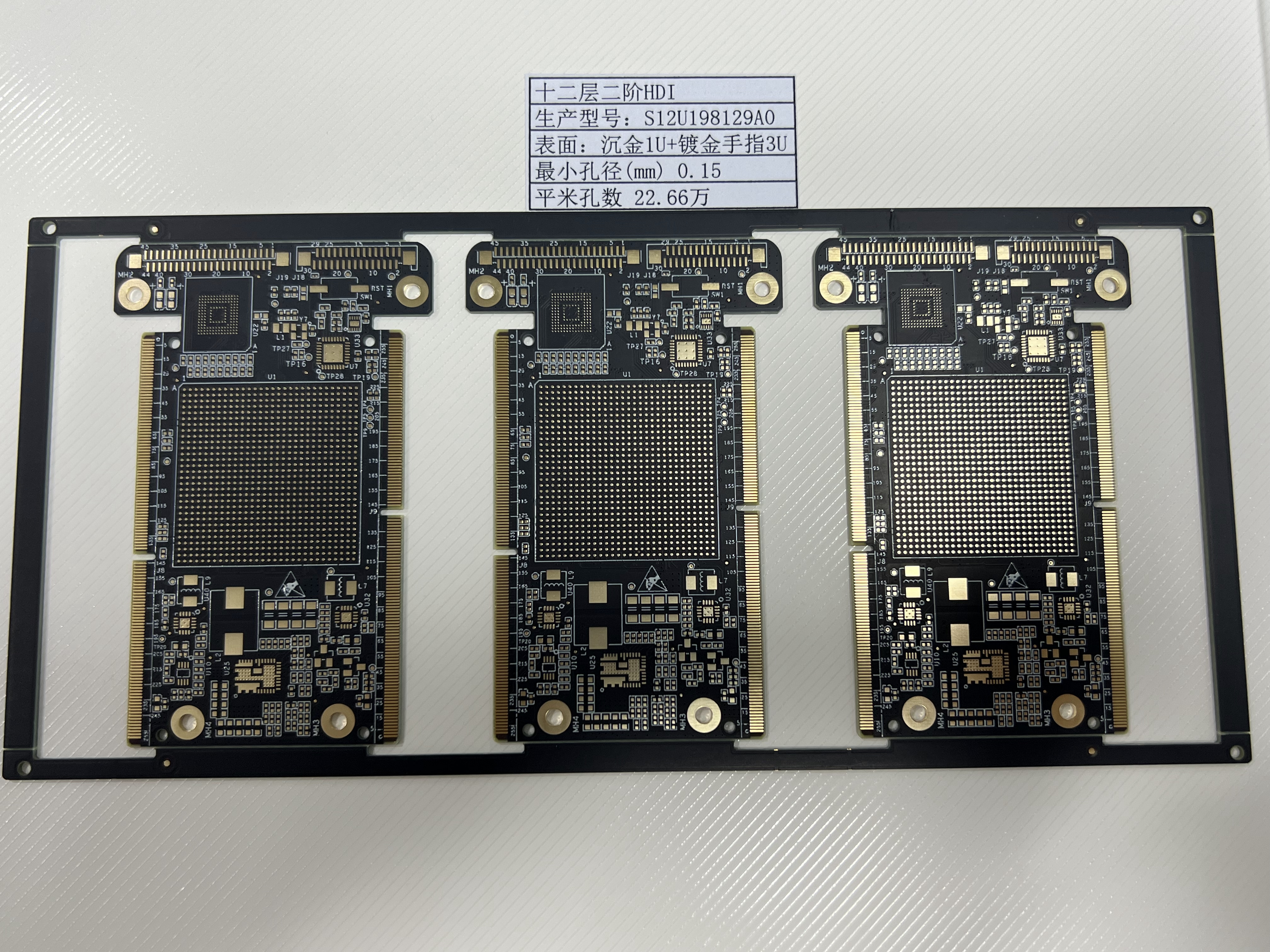
Stackup in HDI PCB Design
A good stackup is very important in HDI PCB Design. It is even more important for high-frequency boards. The stackup shows how copper and dielectric layers are put together. This setup changes how signals move, how many wires fit, and how well the board works. LT CIRCUIT uses smart stackup ideas to help engineers make fast and strong boards.
Layer Configuration
Layer configuration means how many layers the PCB has and how they work together. In HDI PCB Design, engineers use fewer layers than old-style boards. They can do this because of microvias, blind vias, and buried vias. These special vias help save space and fit more wires.
A smart layer setup can make the board 40% smaller and save over 20% in cost.
Metric | Traditional TH Multilayer PCB | Optimized HDI Multilayer PCB | Improvement / Benefit |
|---|---|---|---|
Layer Count | 14 layers | 8 layers | 6 fewer layers |
Board Area | Baseline | 40% less area | Significant area reduction |
Cost Savings (Relative) | Baseline | 20.5% to 28.1% less | Substantial cost savings |
Routing Density (pins/sq. inch) | Baseline | 12X to 20X higher | Dramatic increase in routing density |
Routing Space Increase (via blind vias) | Baseline | 30% more routing space | Enables fewer signal layers needed |
Engineers see that blind vias give about 30% more space for wires inside the board. This helps when there are lots of pins close together, like in BGA chips. Because of this, the number of signal layers can go down by up to 75% for hard boards. This makes the board easier to build and costs less money.
Design studies suggest some best ways to set up layers:
Put ground planes next to every signal layer. This helps signals return and lowers EMI, especially for fast signals.
Place power planes in the middle and close to ground planes. This keeps voltage steady and lowers loop inductance.
Use the outside layers for fast signals. This keeps wires short and cuts down on via jumps for signals above 1 GHz.
Make sure the dielectric thickness is even and pick materials with steady dielectric constants.
Use computer tools to check wire shape and impedance.
Stop crosstalk by making wires farther apart or adding ground shields.
Try new ideas like build-up technology and low-loss materials to make the stackup better.
LT CIRCUIT uses these ideas in their stackup plans. Their engineers use build-up technology and new materials to make small, strong boards. Customers get boards with fewer layers, more wires, and lower costs.
Reference Planes
Reference planes are very important in HDI PCB Design. These planes are usually copper and give a steady voltage for signal layers. They help control impedance, lower noise, and keep signals clear.
Parameter/Aspect | Numerical Value / Description |
|---|---|
Controlled impedance | |
System clock rates | Up to 1 GHz and beyond |
Signal rise/fall times | 0.7 nanoseconds |
Interconnect structure | Multilayer PCBs with buried signal layers between power and ground planes |
Effect of reference planes | Better control of interconnect impedance and decreased instantaneous voltage fluctuations |
Good reference planes help engineers keep impedance steady, which is needed for fast signals. Multilayer PCBs with signal layers between power and ground planes have better voltage and less signal damage. This setup works for clock speeds up to 1 GHz and signal times as quick as 0.7 nanoseconds.
Numbers show why good reference planes help HDI PCB Design:
Metric | Standard PCB (Baseline) | HDI PCB (With Proper Reference Planes) | Performance Gain |
|---|---|---|---|
Component Density | 100% | 400% | |
Layer Count | Up to 8 layers | 20+ layers | 2.5x increase |
Signal Integrity Margin | 80% margin | 95% margin | 15% improvement |
Routing Efficiency | N/A | Improved due to optimized stackup | N/A |
Thermal Resistance | 40-60 °C/W per sq inch | Improved with thermal vias and design | N/A |
LT CIRCUIT always adds good reference planes in their stackups. This gives boards with more parts, better signals, and good heat control. Customers get boards that work with new features and fast speeds.
Tip: Always use at least one solid ground plane and one power plane in your stackup. This helps signals return and lowers EMI.
Engineers who use these stackup ideas in HDI PCB Design see better performance, more trust, and easier building. LT CIRCUIT’s skill in stackup design helps customers get these good results every time.
Signal Integrity
Impedance Control
Engineers must keep impedance steady in high-frequency HDI PCB designs. If impedance is stable, signals move well and do not bounce back. Most boards use 50 ohms for single traces and 100 ohms for differential pairs. Engineers use computer tools before making the board. These tools help them pick the right trace width, spacing, and materials.
Using the same dielectric thickness and a steady dielectric constant (Dk) keeps impedance even.
Putting ground planes next to signal layers helps keep impedance steady.
The width and space of traces depend on the dielectric constant and needed impedance. For example, a 50-ohm trace on FR-4 with Dk near 4.2 often needs to be about 6 mils wide.
After the board is made, engineers check for impedance changes with Time-Domain Reflectometry (TDR). They also use Vector Network Analysis (VNA) to test high-frequency signals and return loss. Test coupons on the board show if the board matches the design.
Tip: Always check impedance with both computer tests and real tests to make sure signals work well.
Crosstalk Reduction
Crosstalk is when signals on close traces mess with each other. Engineers use many ways to stop crosstalk and keep signals clear. Computer tools like SPICE and signal integrity software help find crosstalk before making the board. High-frequency simulators and 3D field solvers show how crosstalk works in detail.
Making more space between signal lines, like from 5 mils to 10 mils, can lower crosstalk a lot.
Shorter runs where traces are side by side also help. Long runs make crosstalk worse.
Using a thin dielectric layer and strip lines instead of microstrip lines helps too.
Eye diagram checks and cross-probing tests show these ideas work on real boards.
The best ways are to make lines farther apart, keep parallel runs short, and put ground planes close to signal layers. These steps help engineers stop crosstalk and keep signals strong in high-frequency HDI PCB designs.
Design Rules
Via Optimization
Engineers make signals better in HDI PCBs by changing via shapes. Microvias are much smaller than normal through-hole vias. They can cut down parasitic inductance by up to 60%. This is very important for signals in the GHz range. Even a little inductance can cause signals to bounce back and get worse. Better via designs also make return paths 30% shorter. They lower the number of layer jumps by 25%. These changes help keep signals strong and lower signal loss.
Benefit Metric | Quantifiable Improvement |
|---|---|
Reduction in via-induced reflections | |
Shorter return paths | 30% shorter in HDI boards |
Fewer layer transitions | 25% fewer in HDI boards |
Reduction in inductance | 60% reduction with microvias |
Yield rate improvement | From 72% to 94% |
First-pass success rate | 98% with via aspect ratio <10:1 |
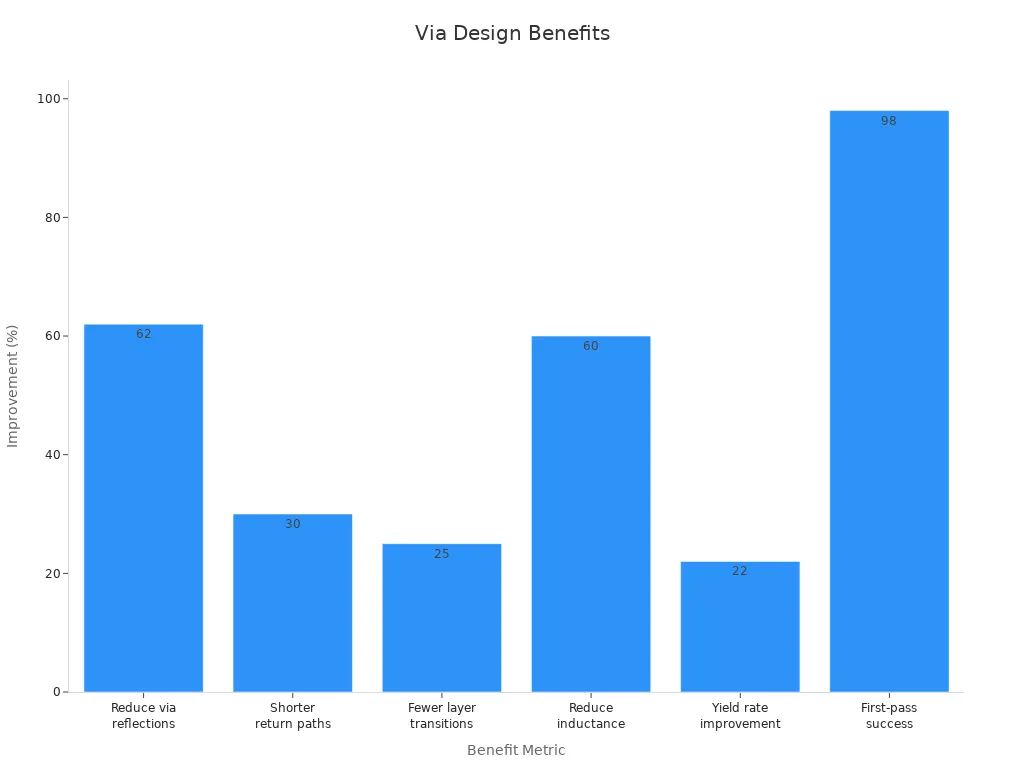
Microvias also help make more boards work right the first time. LT CIRCUIT engineers use these better via ideas to make strong, high-frequency HDI PCBs.
Trace Routing
Good trace routing keeps signals strong in high-frequency boards. Engineers follow some main rules:
Shorter traces help stop signal loss, noise, and crosstalk.
Leaving enough space between traces, at least three times the dielectric thickness, stops signals from mixing.
Keeping trace width the same controls resistance and keeps impedance steady.
Routing important signals first and not putting traces under sensitive parts lowers noise.
Differential pair routing with the same length and even spacing cuts down skew and keeps impedance balanced.
Routing traces in different directions on layers (X on one, Y on the next) lowers capacitive coupling and crosstalk.
Engineers use special tools to figure out crosstalk from trace shapes. Noise margin checks help find out how much crosstalk is okay with other noise. These routing steps, along with better via designs, help LT CIRCUIT make high-quality HDI PCBs for advanced uses.
LT CIRCUIT Solutions
Customization Options
LT CIRCUIT gives many ways to change high-frequency HDI PCB Design. Engineers can pick special materials with low dielectric constants and loss factors, like Megtron 6 or Panasonic R5775. These help keep signals strong when data moves fast. The company can make very small holes, as tiny as 0.1mm. They also make thin lines and spaces, down to 3mil/3mil. Copper can be thick or thin, from 0.5oz to 6oz. This helps control heat and how much current the board can handle. Customers can choose board thickness from 0.2mm to 6.0mm. They can also pick different solder mask colors for their needs.
LT CIRCUIT’s HDI Any Layer PCBs let engineers set up layers in the best way. They can use controlled impedance routing and special via designs, like microvias and backdrilling. These things help lower signal loss, make boards smaller, and make them work better. The company checks boards with tests like Flying Probe Test and E-test to make sure they work right. These choices help in tough jobs, like medical devices, car sensors, planes, and electronics people use every day.
Quality Assurance
LT CIRCUIT works hard to give good quality, new ideas, and happy customers. The company uses strong quality checks at every step:
They follow world rules like ISO 9001, UL, and CE.
They use Automated Optical Inspection (AOI) and X-ray checks to find problems, cutting defects by up to 40%.
They test for heat and if the board works, including thermal cycling and impedance checks.
They check boards many times to make sure quality is high.
They meet IPC-610 Class 3 standards.
They make boards without lead and follow RoHS rules.
They use SPC, AI models, and Digital Twin Technology to keep getting better.
They use LTspice and Monte Carlo analysis to check signals in real life.
These steps make sure every HDI PCB Design is strong and works well. LT CIRCUIT’s smart checks and tests stop up to 85% of signal loss problems. This helps them give great, high-frequency PCB solutions.
Challenges and Tips
Material Sourcing
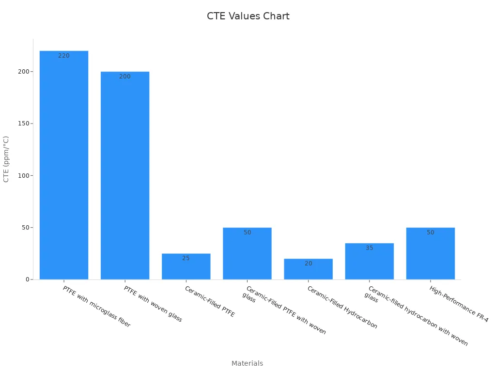
Engineers have many problems when getting materials for high-frequency HDI PCB designs. They need to think about how well the board works, how strong it is, and how much it costs. Each material has its own good and bad points. Making one thing better can make another thing worse. For example, a material with a low dielectric constant (Dk) might not stick well or handle heat changes.
Material datasheets do not always have all the right facts. This makes picking the best material hard.
Sometimes teams forget to check laminate properties early. This can cause mistakes and slow down the project.
High-performance boards need materials that do not change shape with heat, stick well, and stay strong. But these things can make the board cost more.
Getting the right materials means working well with suppliers and planning carefully.
Parameter / Material Aspect | Description / Quantitative Data |
|---|---|
Dielectric Constant (Dk) | It must stay steady at different frequencies. The value changes with each material. PTFE is 2.1-2.55. FR-4 is 4.2-4.5. |
Loss Tangent (Df) | It should be low, under 0.004, or even 0.001. This helps keep signals strong and stops too much heat. |
Thermal Conductivity | High thermal conductivity helps move heat away. This is different for each material. |
Coefficient of Thermal Expansion (CTE) | If CTE does not match, the board can crack or vias can break. |
PTFE works best but costs more and is harder to use. Hydrocarbon materials are cheaper and work pretty well. |
Tip: If design and buying teams talk early, they can pick the right material and avoid mistakes that cost money.
Manufacturing Constraints
Making high-frequency HDI PCBs is not easy. Engineers must follow strict rules for trace width, spacing, and via sizes. This keeps signals working right. Even small mistakes or problems can make signals weak or cause the board to fail.
Parameter | Description |
|---|---|
Dielectric Constant (Dk) | Dk must be low and steady to keep impedance the same. |
Dissipation Factor (Df) | Lower Df means less signal loss and better signals. |
Thermal Expansion (CTE) | If CTE does not match, the board can break. Matching CTE helps the board last longer. |
Impedance Control | Trace width, spacing, and stack-up must be just right to keep impedance steady. |
Via Sizes and Effects | Placing vias carefully and using fewer helps signals stay clear. |
Trace Width and Spacing | These must be right for the board to carry current and keep impedance. |
Stack-up Configurations | How layers are stacked changes impedance and blocks noise. |
Making microvias and plating copper needs special machines and skilled workers.
Checks like AOI and X-ray help find problems before they hurt signals.
Using DFM tools and talking to the factory early helps make boards that work well.
Note: Engineers who work with factories and use DFM tools can stop problems and make sure signals stay strong.
Picking the right materials and stackup is very important. These choices affect how well high-frequency HDI PCB Design works. LT CIRCUIT gives smart solutions and good advice. Their team helps engineers get strong and steady results. Engineers can talk to LT CIRCUIT or other experts for help that fits their needs.
FAQ
What materials work best for high-frequency HDI PCB designs?
Engineers like to use PTFE, Rogers, and Megtron 6. These materials have low dielectric loss. They also work well at high frequencies.
How does stackup affect signal integrity in HDI PCBs?
A good stackup helps stop signal loss and crosstalk. It also makes impedance control better. LT CIRCUIT uses smart stackup plans for the best results.
Can LT CIRCUIT customize HDI PCBs for unique project needs?
Yes, LT CIRCUIT lets you pick special materials, layer numbers, and via types. Their team helps with special needs for advanced projects.
See Also
Essential Design Tips For Manufacturing Reliable HDI PCBs
Evaluating Costs And Benefits Of Advanced HDI Microvia Designs
A Guide To Common Stack-Up Configurations In HDI Multilayers
Design And Production Insights For High Frequency RF PCBs
Learn Cutting-Edge Methods For Prototyping Advanced HDI PCBs