How HDI PCB Laser Hole Via Filling Works
HDI PCB laser hole via filling is very important today. It closes vias to stop solder leaks and makes connections stronger. It also helps spread heat better. Microvias are smaller than regular vias. They let PCBs have more layers without getting bigger. This helps make small devices like smartphones and IoT gadgets.
Key Takeaways
HDI PCB laser hole filling improves connections and stops solder leaks. This makes devices work better and last longer.
Microvias help make smaller designs. They let makers add more parts in tiny spaces, great for today’s gadgets.
Laser drilling makes exact holes. This boosts signal strength and cuts down interference, which is key for fast devices.
Understanding HDI PCB Laser Hole Via Filling
What is HDI PCB Laser Hole Via Filling?
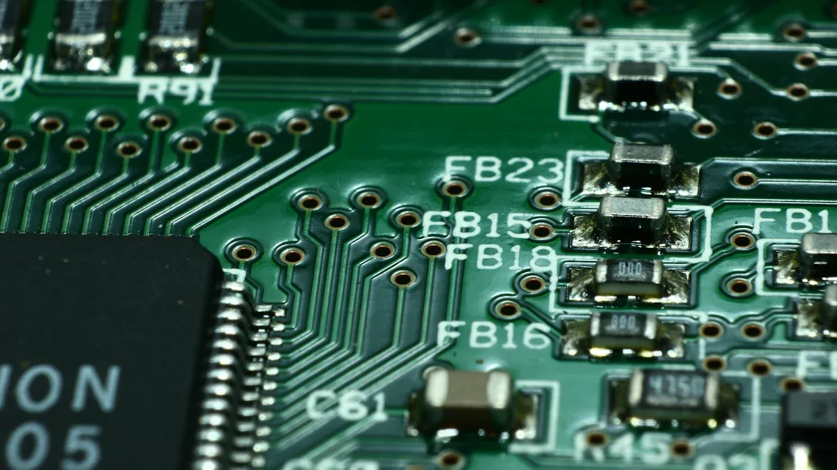
HDI PCB laser hole via filling is a special method. It fills microvias in high-density interconnect (HDI) PCBs with conductive materials. Microvias are tiny holes, about 80-100 µm wide, that link PCB layers. This process ensures strong electrical connections and stops solder from leaking. It also helps spread heat better. Using laser drilling and advanced filling methods, manufacturers create accurate results for modern electronics.
Specification | Value |
|---|---|
Diameter of laser hole | 80-100 µm |
Dielectric thickness | 60-80 µm |
Importance of process combination | Ensures reliable welding and thermal dissipation |
Laser drilling is very important in this process. It makes clean, precise holes to keep the PCB strong. The filling step adds resin or copper into these holes. This creates a smooth surface for the next steps. Together, drilling and filling improve the PCB's strength and performance.
The Role of Microvias in HDI PCBs
Microvias are key to making HDI PCBs work. Their small size allows compact and efficient designs. These tiny holes shorten signal paths, reduce signal loss, and improve signal quality. They also allow more connections in less space, perfect for dense designs.
Aspect | Impact of Microvias |
|---|---|
Via Stubs | Reduced, enhancing signal integrity |
Signal Path Length | Shortened, leading to reduced reflections |
Attenuation | Lowered due to improved routing |
Microvias save space and lower costs. They let you fit more parts into smaller areas, cutting manufacturing expenses. They also reduce electromagnetic interference (EMI) by shrinking potential antennas. This makes HDI PCBs great for smartphones, wearables, and IoT devices.
Benefit | Explanation |
|---|---|
Microvias enable denser connections and smaller traces, essential for fitting fine-pitch components. | |
Improved Signal Integrity | Smaller parasitic capacitance and inductance enhance signal integrity, minimizing high-speed issues. |
Reduced EMI | Microvias, being smaller, reduce the size of potential antennas, leading to less signal radiation. |
Key Steps in the Laser Hole Via Filling Process
The laser hole via filling process has several steps. Each step ensures the final product is reliable and efficient.
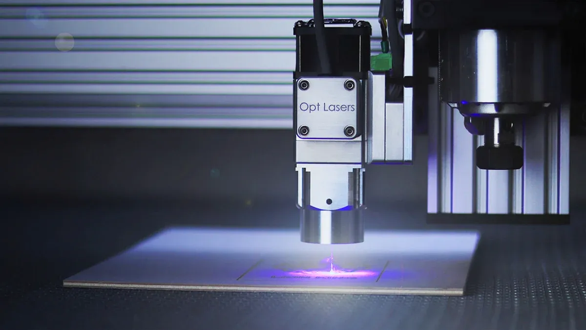
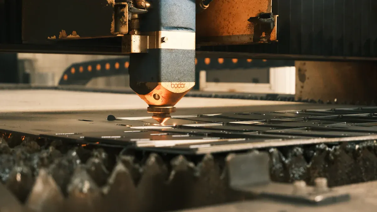
Drilling: Lasers make tiny, accurate holes. These holes go through layers without damaging nearby areas.
Cleaning: The holes are cleaned to remove dirt and debris. This makes the surface smooth for the next steps.
Preparation for plating: A thin copper layer is added inside the holes. This helps create electrical connections.
Plating: Copper is electroplated onto the walls of the holes. This forms a conductive path.
Filling with resin: Resin is pushed into the holes under pressure. This removes air gaps and fills them evenly.
Planarization: Extra resin is removed, leaving a flat surface ready for soldering.
Studies show these steps improve quality. For example, roll-to-roll methods increase yield and lower resistance. Techniques like plasma etching and UV laser ablation make surfaces smoother and more precise.
Method | Efficiency | Impact on Quality |
|---|---|---|
Plasma etching | High | |
CO2 laser ablation | Medium | Effective patterning |
UV laser ablation | High | Precise control over dimensions |
By following these steps, HDI PCBs become stronger and better. They are perfect for advanced uses.
Benefits of HDI PCB Laser Hole Via Filling
Better Electrical and Mechanical Features
HDI PCB laser hole via filling makes boards work better. Filling microvias with copper or resin helps electricity flow smoothly. This improves signals, reduces loss, and boosts speed. Filled vias also spread heat well, keeping the board cool.
This process makes PCBs stronger. It lowers the chance of breaking from stress or weather. Filled vias also make soldering easier and reduce mistakes. These benefits make HDI PCBs great for complex circuits and advanced uses.
Performance Metric | Benefit |
|---|---|
Stronger Boards | |
Better Signal Quality | Signals stay clear and lose less strength. |
Heat Control | Spreads heat evenly to keep the board cool. |
Easier Soldering | Reduces mistakes during assembly. |
Extra Support | Helps parts stay in place and handle shocks. |
Perfect for Compact Designs
Laser hole via filling helps make small, multi-layered boards. Microvias allow more layers without making boards bigger. This is important for devices like phones and IoT gadgets, where space is tight. The process also stops solder from leaking, keeping connections strong.
Laser drilling is key to this process. It creates tiny, accurate holes for microvias. These holes shorten signal paths, improving signal quality and reducing interference. This makes HDI PCBs ideal for modern, compact designs.
Why It’s Better Than Older Methods
HDI PCB laser hole via filling has many advantages over older ways. Laser drilling makes smaller, more exact holes than mechanical drilling. This helps shrink circuit boards. Filling vias stops solder problems, making circuits more reliable.
Though it costs more, the benefits are worth it for high-tech uses. Better signals, space-saving designs, and durability make it a smart choice. Industries like aerospace and medical devices need this advanced method.
Key benefits include:
Stops solder leaks for reliable connections.
Worth the cost for better performance and compact designs.
Using this process helps create top-quality PCBs for modern electronics.
Applications of HDI PCB Laser Hole Via Filling
Consumer Electronics and Smartphones
You use gadgets like smartphones and tablets every day. These devices need small, powerful PCBs to work well. HDI PCBs, improved by laser hole via filling, help make these devices smaller and faster. This process lets manufacturers add more parts in less space using microvias.
Laser-drilled microvias improve signals and shrink board size. This is very important for smartphones, where space is limited. Via-in-pad designs save even more space and boost speed.
Benefits for smartphones include:
Laser-drilled microvias improve PCB performance.
Via-in-pad designs make boards smaller.
These methods ensure reliable and fast devices.
The need for HDI PCBs in electronics keeps growing. Better laser drilling and via filling meet the demand for smaller devices. Technologies like 5G and IoT also need faster and stronger communication systems.
Feature | Benefit |
|---|---|
Microvias | Allow multi-layer designs |
Space Saving | Fit more parts in less space |
Performance | Keep devices working well |
Automotive and Aerospace Innovations
Cars and airplanes need precise and reliable systems. HDI PCBs with laser hole via filling meet these needs. They are used in features like collision avoidance and aerospace controls. These PCBs work well even in tough conditions like heat and vibrations.
Fiber lasers make better holes for aerospace systems. Studies show fiber lasers are better than older Nd:YAG lasers. Techniques like trepanning improve hole shapes and reliability.
Year | Special Boards Output Value | Percentage of Total | |
|---|---|---|---|
2007 | $50.9 billion | $2.3 billion | 4.5% |
2014 | 170 billion RMB | 10.2 billion RMB | 6.0% |
In cars, HDI PCBs support advanced systems like self-driving and entertainment. Tests show via-filled PCBs resist cracking, vibrations, and moisture. For example:
Thermal tests (-55°C to 125°C) show strong PCBs.
Vibration tests confirm better stability.
Moisture tests prove epoxy-filled vias resist damage.
Test Type | Condition Simulated | Performance Metric | Benefits of Via Technologies |
|---|---|---|---|
Thermal cycling | -55°C to 125°C for 1,000 cycles | Resists cracking/delamination | Via filling spreads heat evenly |
Vibration testing | Frequency range 10-2,000 Hz | Strong via-in-pad structure | Better mechanical stability |
Moisture exposure | High humidity environments | Prevents delamination | Epoxy-filled vias resist moisture |
Medical Devices and Wearables
Medical tools and wearables need accuracy and reliability. HDI PCBs with laser hole via filling deliver both. In medical devices, laser drilling makes tiny, precise microvias. For example, osmotic pumps use small holes to control medicine release. Laser drilling ensures these holes are accurate and consistent.
Wearables like fitness trackers and smartwatches also use HDI PCBs. These devices need small, high-performing PCBs to work well. Laser hole via filling allows more connections, better signals, and improved heat control. This keeps wearables small but powerful.
Advantage | Description |
|---|---|
Higher Routing Density | Fits more connections in less space. |
Better Signal Quality | Shorter paths improve signal strength. |
Improved Heat Control | Helps parts stay cool. |
Smaller Boards | Allows smaller designs with more features. |
Better Component Placement | Makes placing parts easier and more efficient. |
Stronger Connections | Improves solder joint reliability. |
High-Frequency Use | Works well for fast signals due to shorter paths. |
Laser-made circuits also make wearables more reliable. Microvia designs help shrink devices while keeping them efficient. As wearables improve, HDI PCBs with laser hole via filling will remain essential.
HDI PCB laser hole via filling is very important today. It helps make small designs that work better and last longer. LT CIRCUIT is a leader in creating smart HDI PCB solutions. These solutions meet the needs of industries like electronics and cars. Future HDI PCB technology will bring new ideas and improvements. Tiny PCBs will keep helping wearables, medical tools, and car systems grow and improve.
FAQ
Why is HDI technology important for today's electronics?
HDI technology helps make smaller designs with better signals. It is used in powerful devices like phones, wearables, and medical gadgets.
How does laser drilling make PCBs better?
Laser drilling makes tiny, exact holes called microvias. These holes create strong links and reduce signal problems. It also makes PCBs tougher.
Are HDI PCBs good for high-frequency signals?
Yes, HDI PCBs are great for high-frequency signals. Shorter paths and filled holes keep signals clear and reduce interference.
See Also
Achieving Flatness in HDI PCB Laser Drilling Holes
Understanding Back Drilling Techniques in HDI PCB Production
Designing and Producing Any Layer HDI PCBs Effectively