HDI PCB Manufacturing: Key Design Considerations for Reliable High-Density Interconnect Boards
Reliability in HDI PCB manufacturing begins with smart planning. These special PCBs help build smaller, quicker, and better gadgets. LT CIRCUIT excels in producing top-quality boards using innovative ideas and precision. Choosing their team means collaborating with experts who create robust, high-speed HDI boards.
Key Takeaways
Focus on keeping signals clear by reducing interference and noise. Use materials that lower signal loss and keep paths apart. This helps the board work better.
Make sure power flows steadily with a good design. Put small capacitors close to power pins to keep voltage steady.
Keep signal paths balanced to prevent problems. Use even trace widths and spacing. Work with manufacturers to match the right materials.
Signal and Power Integrity in HDI PCB Manufacturing
Minimizing Crosstalk and Noise
Crosstalk and noise can hurt how well HDI PCBs work. This is especially true for fast-moving signals. To fix this, keep conductive paths spaced apart and use materials with lower dielectric constants. Shorter coupled lengths also help reduce interference.
Lower dielectric constant materials and shorter lengths cut crosstalk by 50%.
Thin dielectric layers reduce crosstalk and lower inductance and capacitance.
These methods can shrink board size by 28%, making designs smaller and better.
Using these ideas ensures your HDI PCBs work reliably and perform well.
Ensuring Stable Power Delivery
Stable power is key for keeping signals strong in HDI PCBs. Without it, circuits may fail or have voltage drops and noise. To prevent this, design a good power distribution network (PDN).
Set clear rules for vias and pads to keep connections steady. Managing heat is also important for stable power. Too much heat can block current flow, so pick materials that handle heat well.
Tip: Place decoupling capacitors near power pins. This lowers noise and keeps voltage steady. It’s a simple way to make HDI PCBs more reliable.
Routing Guidelines for High-Speed Signals
Routing fast signals in HDI PCBs needs careful planning. Good routing keeps signals clean and avoids problems like reflections or interference.
Here’s a table showing key layout tips and why they matter:
Metric | Why It Matters |
|---|---|
Impedance Control | Keeps signals steady over distance, reducing losses and reflections. |
Stops crosstalk by keeping traces far enough apart. | |
Signal Return Path Issues | Prevents noise and interference by routing return paths correctly. |
Follow these tips to improve HDI PCB performance. For example, spacing traces properly reduces crosstalk. Impedance control keeps signals clear. These steps are vital for making reliable HDI PCBs.
Controlled Impedance for Reliable HDI PCBs
Why Impedance Matching Matters
Matching impedance is important for making HDI PCBs work well. When signals move through a PCB, mismatched impedance can cause signal echoes. These echoes distort signals and hurt high-speed circuit performance. So, controlling impedance keeps signals clear and reliable.
Matching impedance stops extra noise in digital signals.
It lowers unwanted emissions, helping meet EMC rules.
PCB size and materials affect impedance, so design carefully.
Tip: Work with your manufacturer to match material thickness and copper height to your design. This avoids impedance issues and keeps performance steady.
How to Control Impedance
To control impedance, you need accurate designs. At high speeds, PCB traces act like signal paths. If impedance changes along these paths, signals can get distorted. Keeping impedance the same avoids these problems.
Here are some ways to do it:
Keep trace widths and spacing the same: Small changes can mess up impedance.
Pick the right materials: Materials affect impedance based on their properties.
Test designs with tools: Simulations can show how impedance will behave.
For example, using the same trace width and thickness keeps signals clear. This reduces echoes and improves signal quality. Manufacturers also check material thickness to match designs, making boards more reliable.
Avoiding Design Mistakes
Designing for controlled impedance can be tricky, especially for HDI PCBs. Mistakes can delay production or cause poor performance.
Uneven trace widths can distort or weaken signals.
Confusing specs, like different trace widths on one layer, can stop production.
Wrong trace spacing or thickness can ruin signal quality.
To avoid these mistakes, follow these tips:
Set clear rules for each PCB layer.
Work with your manufacturer to match designs with their tools.
Use one trace width per layer to avoid confusion.
Fixing these issues early makes production faster and ensures HDI PCBs work well.
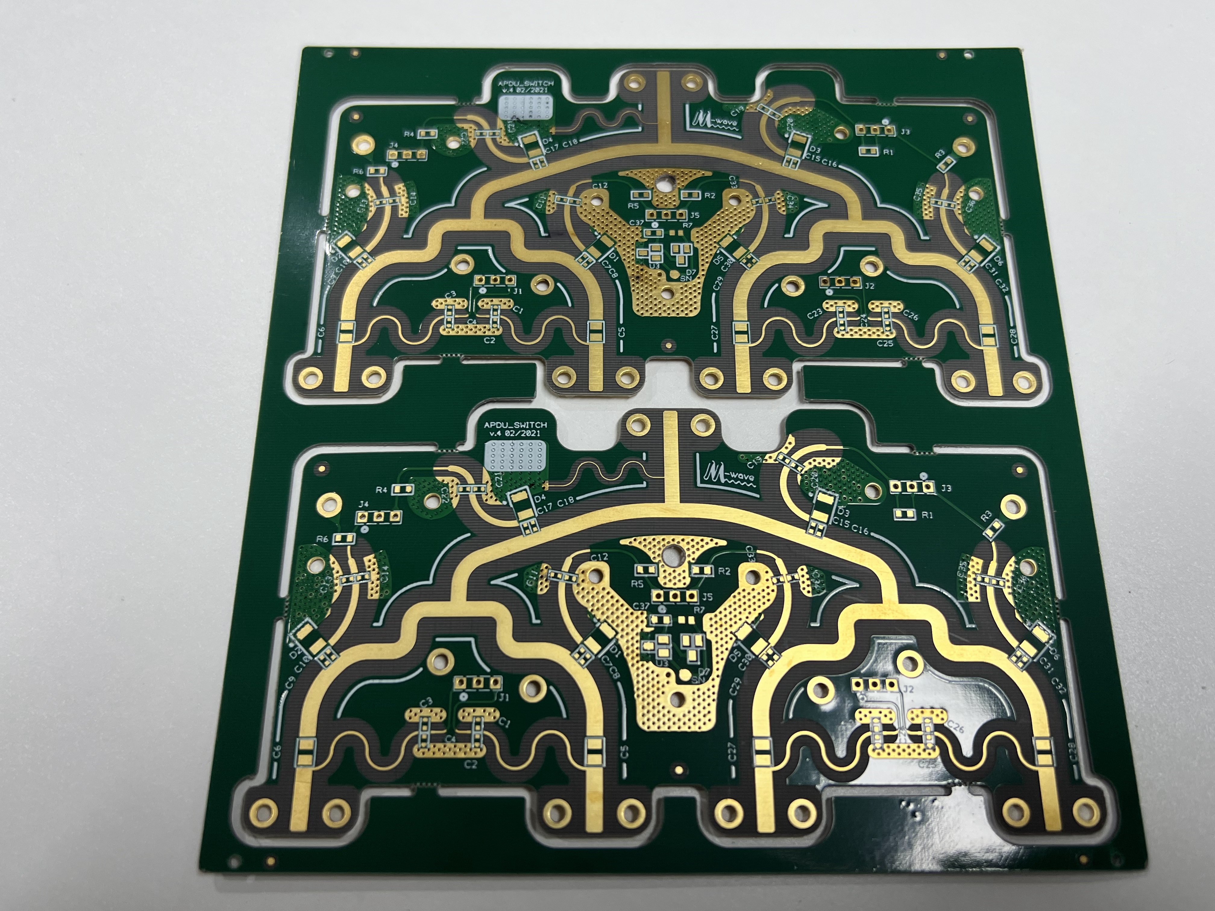
Layer Stack-Up Design for HDI PCBs
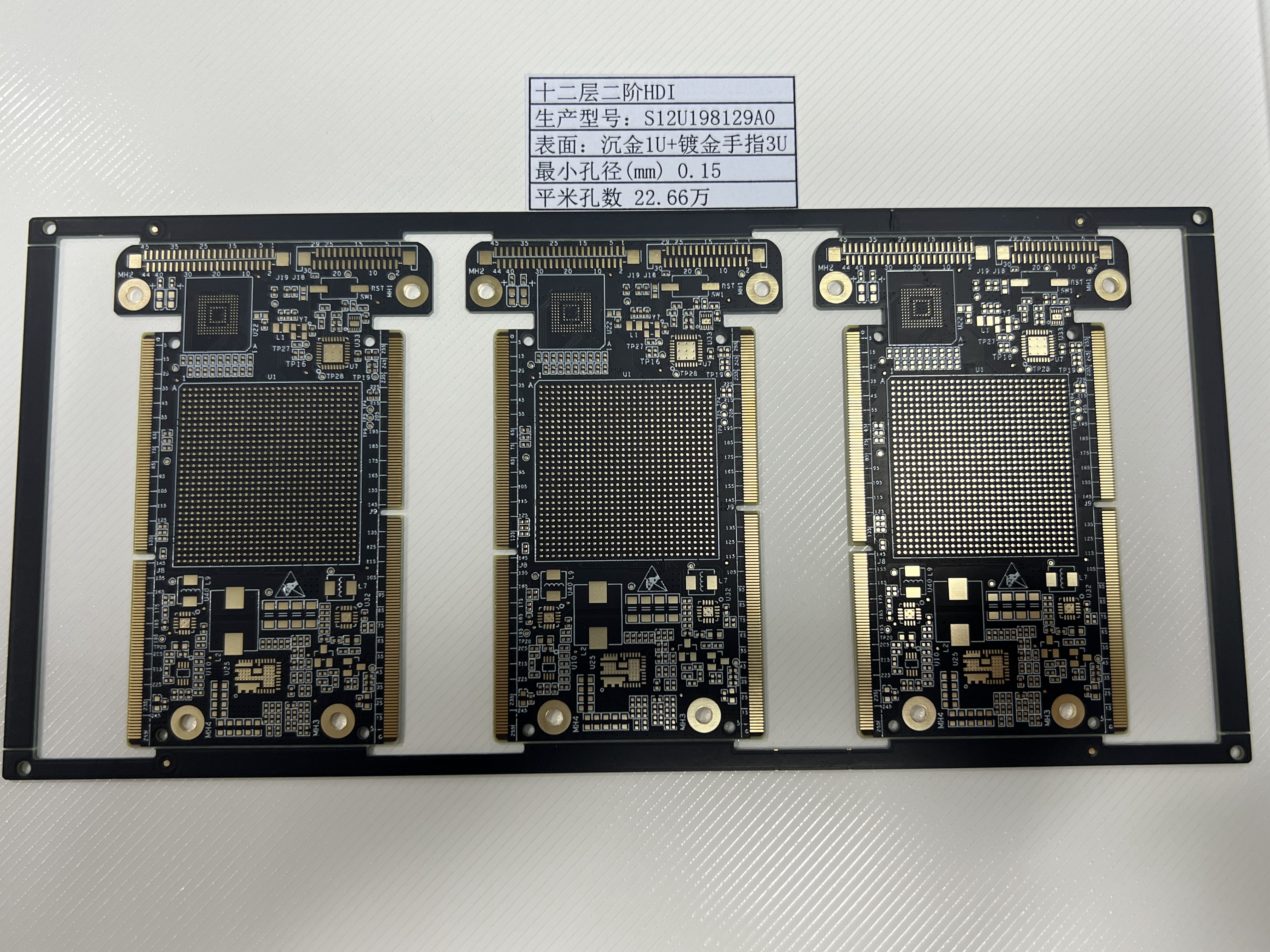
Optimizing Layer Count and Stack-Up
Picking the right number of layers is very important. Most HDI PCBs use 4 to 12 layers, depending on the circuit's complexity. Balancing copper weights across layers makes boards stronger. This helps prevent bending during manufacturing.
Simplify designs by reducing extra layers. Fewer layers can remove the need for blind vias. This makes boards easier to build and lowers costs. It also improves production success rates.
Tip: Work with your manufacturer to choose the best layer count. This keeps your design efficient and easy to produce.
Balancing Signal Layers and Ground Planes
Signal layers and ground planes must be balanced for good performance. Ground planes protect signals and stop interference. This is very important for fast circuits where small signal loss matters.
Good stack-up designs also improve power flow. Ground planes reduce voltage drops and keep power steady. They also help cool the board by spreading heat evenly.
Key Insight: Use separate ground and power planes. This lets signal layers focus on routing and improves overall performance.
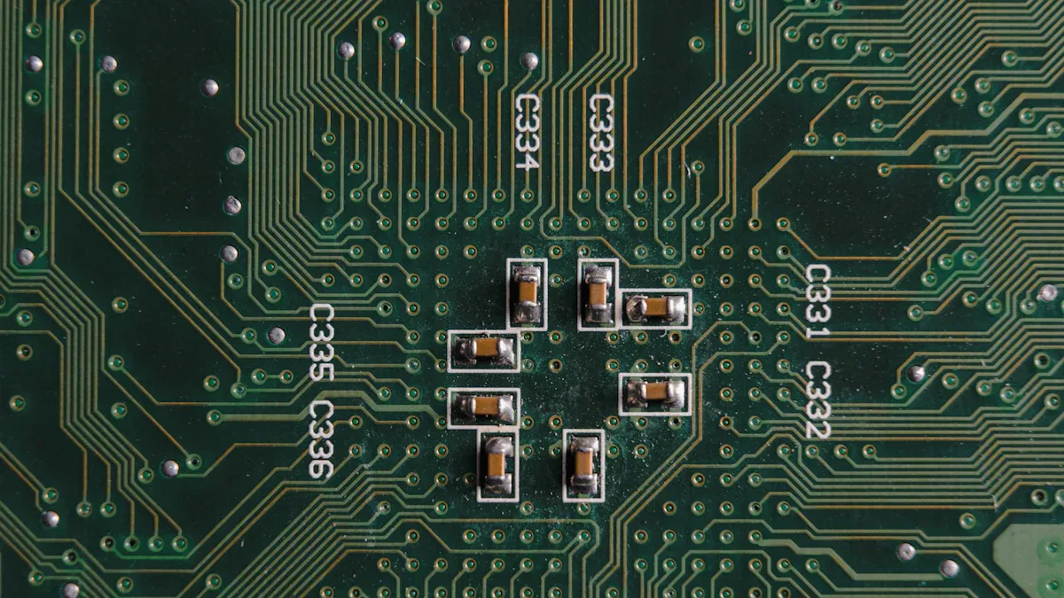
Best Practices for Via Placement
Vias connect layers in HDI PCBs and must be placed carefully. Too many vias in one spot can weaken the board. Spread them out to keep the board strong.
Microvias are great for saving space and allowing more connections. But don’t let vias block signal paths or power flow. Proper placement avoids signal problems and makes the board last longer.
Pro Tip: Use staggered or stacked microvias to save space while keeping the board reliable.
Thermal Management in HDI PCB Manufacturing
Handling Heat Challenges
Managing heat in HDI PCB designs is very important. Small boards and packed circuits make heat hard to control. Using smart heat management methods keeps the board working well.
Packed circuits create more heat in tiny spaces.
Materials that move heat quickly and cooling methods are needed.
Thermal vias help remove heat from the board. Put them under parts that make heat. This gives heat an easy way out. It stops overheating and helps the board last longer.
Picking Materials for Better Heat Control
The materials you choose affect how well heat is handled. Regular PCB materials don’t move heat as well as copper. Copper moves heat much faster, making it a better choice.
Copper layers, pads, and traces guide heat to cooler areas. These materials help keep the board cool. Picking good materials keeps the board steady even with lots of power.
Using Thermal Vias and Heat Sinks
Thermal vias and heat sinks are great for cooling HDI PCBs. Thermal vias add more copper to the board, lowering heat resistance. They move heat away from hot parts to cooler areas.
Heat sinks spread heat out by adding more surface area. They cool parts like chips by pulling heat away. Using both thermal vias and heat sinks makes a strong cooling system. This keeps the board cool and working well under tough conditions.
Tip: Add thermal vias and copper under hot parts when designing. This stops heat problems before they happen.
Manufacturing Constraints and Collaboration with LT CIRCUIT
Design for Manufacturability (DFM) Guidelines
Making HDI PCBs easy to produce is very important. Simplify designs to avoid extra features that make production harder. Keep trace widths and spacing the same to prevent mistakes.
Working with LT CIRCUIT gives you expert help with DFM. Their team checks your designs to find problems early. Fixing issues ahead of time avoids delays and keeps quality high. Using DFM rules makes production faster and results better.
Understanding Fabrication Limitations
Manufacturing has limits, and knowing them helps HDI PCB success. Microvias need the right size and shape to work well. Too many parts or vias in one spot can weaken the board.
LT CIRCUIT uses advanced tools to handle these limits. Their flying probe testers check circuits for problems like shorts or breaks. These tools are fast and precise, even for tricky designs. This ensures your boards work as planned.
Benefits of Partnering with LT CIRCUIT for HDI PCB Manufacturing
LT CIRCUIT offers many benefits for HDI PCB projects. Their services save time and improve quality. They place tiny parts with 99.5% accuracy, ensuring great results. Their boards meet global standards for reliability.
Here’s how flying probe testing helps production:
Key Advantages of Flying Probe Tester | Description |
|---|---|
Efficiency | Tests many connections quickly, speeding up production. |
Precision | Finds tiny electrical problems, keeping quality high. |
Versatility | Handles tests like continuity and short-circuit checks. |
Automation | Reduces human errors with automatic testing. |
Wide Applicability | Works for different PCB sizes and designs. |
Reliability | Spots issues early, improving product performance. |
Cost-Effectiveness | Prevents expensive recalls or fixes later. |
Partnering with LT CIRCUIT gives you top tools and knowledge. This teamwork makes HDI PCB production smooth and cost-effective.
Making reliable HDI PCBs starts with smart design choices. Clear signals need good impedance control and signal planning. Proper layers and heat control stop problems like overheating or noise. Working with LT CIRCUIT makes production easier. Their all-in-one service ensures designs follow rules and work well every time.
FAQ
What makes HDI PCBs special compared to regular PCBs?
HDI PCBs use microvias and thin layers to fit more parts. This helps make smaller and faster electronic devices.
How do you keep signals clear in HDI PCBs?
Follow simple routing rules and control impedance carefully. Add decoupling capacitors to reduce noise and keep signals strong.
Tip: Work with LT CIRCUIT for expert design help.
Why is heat control important in HDI PCB designs?
Tightly packed circuits create heat that can harm parts. Use thermal vias, heat sinks, and good materials to keep the board cool.
🔥 Note: Copper layers are great for spreading heat quickly.
See Also
Explore Cutting-Edge Techniques for HDI PCB Prototyping
Understanding the Design and Production of HDI PCBs
Effective Ways to Reduce Back Drilling Costs for HDI PCBs