High-Density Interconnect in Multilayered PCBs and LT CIRCUIT's Advanced Manufacturing Capabilities
High-Density Interconnect technology helps engineers fit more parts on both sides of a multilayered PCB. This makes electronic devices smaller, faster, and more reliable. The global HDI PCBs market was worth $12.5 billion in 2023. This growth happened because of demand in smartphones, cars, and 5G communications.
Aspect | Statistic / Finding |
|---|---|
USD 12.5 billion | |
Projected Market Size (2032) | USD 23.8 billion |
Key Growth Drivers | Miniaturization, enhanced device functionality |
LT CIRCUIT leads in new ideas. They offer advanced solutions for high-performance and small circuit boards.
Key Takeaways
High-Density Interconnect (HDI) technology helps engineers put more parts on small circuit boards. This makes things like smartphones and medical tools smaller. It also makes them faster and more reliable.
LT CIRCUIT uses special methods like laser drilling. They also use strict quality checks. This helps them make strong and accurate HDI PCBs. These PCBs meet hard industry rules. They also help customers get products ready faster.
HDI PCBs are important in many fields like cars, healthcare, and airplanes. They help devices work better and last longer. They also make devices smaller. HDI PCBs support new and hard designs.
High-Density Interconnect Overview
What is HDI?
High-Density Interconnect, or HDI, is a kind of printed circuit board. It lets engineers put more parts in a small area. HDI PCBs have special things like microvias, blind vias, and buried vias. Microvias are tiny holes that are less than 150 microns wide. They connect different layers of the board. Blind vias join the outside layers to the inside ones. Buried vias only link the inside layers together. These features help make devices thinner, lighter, and stronger.
HDI technology has changed how electronics are made. It helps make devices like smartphones, tablets, and wearables smaller. The market for multilayer PCBs with 8 to 10 layers or more is growing. This is because people want more parts in less space and better signals.
Aspect | Details |
|---|---|
Typical Microvia Size | Less than 150 microns |
Trace Width/Spacing | 100 microns or less |
Key Standards | IPC-2315, IPC-2226, IPC-4104, IPC-6016 |
Main Applications | Mobile phones, automotive electronics, 5G, IoT, high-speed computing |
Key Features
HDI PCBs are special for many reasons:
Microvias give strong and exact links between layers.
Blind and buried vias save space and help electricity flow better.
Coreless boards are thinner and can bend more.
Small traces and tiny vias let more parts fit on the board.
Many companies use HDI to make devices with more features in smaller sizes. For example, new smartphones and fast computers need HDI PCBs for speed and trust. HDI boards also cut down on noise and crosstalk. This makes signals better and devices work well.
HDI in Multilayered PCBs
Structure and Design
Engineers use High-Density Interconnect to make multilayered PCBs with special features. These boards have microvias, blind vias, and buried vias. Microvias join layers but do not need much space. Blind and buried vias help signals move between layers. Designers add layers one at a time using build-up construction. This way, the board can be more flexible and have harder circuits.
The table below lists important design rules and what they do in HDI multilayered PCBs:
Design Specification / Metric | Description / Role |
|---|---|
Signal Integrity | Careful planning of interconnections to minimize interference and signal loss. |
Thermal Management | Prevents overheating and keeps components reliable. |
Component Placement | Strategic layout for better routing and electrical performance. |
Routing Complexity | Microvias and stacked microvias allow for intricate routing. |
Build-Up Construction | Adds layers sequentially for more flexibility and density. |
Coreless Construction | Removes solid cores, making boards thinner and more flexible. |
Manufacturing Techniques | Uses laser drilling and precise material deposition for microvias. |
Performance Advantages
High-Density Interconnect in multilayered PCBs gives many good things. Devices get smaller and lighter. Engineers can put more parts in a small space. This helps smartphones, wearables, and medical devices work better. HDI makes signals stronger, so data moves faster and with less noise. Good thermal management keeps devices cool and working well. Microvias and smart routing lower electrical problems. These features help products last longer and work better.
Tip: HDI multilayered PCBs are used in aerospace and medical electronics because they are very reliable and strong.
Manufacturing Challenges
Technical Complexities
Engineers have many problems when making HDI PCBs. These boards are very small and packed with parts. Making them needs special steps and careful work. Tiny traces and microvias must be made just right. Stacked layers need to fit together perfectly. If there is a small mistake, the board might not work.
Some main problems are:
Miniaturization means making devices smaller but still strong.
High-precision patterns need skilled workers and good tools.
New packaging, like 2.5-D and 3-D, adds more layers and links.
Designers must think about trace density, via types, and how long the board lasts.
Aspect | Description |
|---|---|
Making devices smaller but keeping them strong | |
Manufacturing Complexities | Needing careful work for boards with many layers |
Advanced Packaging | 2.5-D and 3-D packaging makes boards more complex |
Design Considerations | Balancing trace density, via types, and reliability |
Industry standards like IPC-2315 and IPC-2226 help engineers with these hard steps.
Quality and Reliability
Quality and reliability are very important for HDI PCBs. Makers test each board to make sure it works well. They check if the board can handle heat and if all paths connect right. Automated Optical Inspection (AOI) finds problems early.
Main quality steps are:
Testing heat and electricity to check performance
Using AOI to spot problems
Watching the process to catch mistakes fast
Using SPC to keep results the same
In-circuit and flying probe tests for full checks
Makers also use ISO 9001 systems and train workers to keep quality high. Risk checks help find and fix problems before boards go to customers. These steps help HDI PCBs stay strong in tough jobs.
LT CIRCUIT Capabilities
Advanced Processes
LT CIRCUIT uses new ways to make printed circuit boards. They use laser drilling to make microvias and stacked vias very accurately. Automated Optical Inspection, X-ray checks, and flying probe tests help find problems early. These steps make sure the boards are safe and work well in important devices.
LT CIRCUIT picks good materials for every job. The team uses special copper, advanced laminates, and strong solder masks. These materials help the boards handle heat and keep signals clear. The company follows strict rules like ISO 9001 and ISO 13485. These rules show LT CIRCUIT meets world standards for quality and safety.
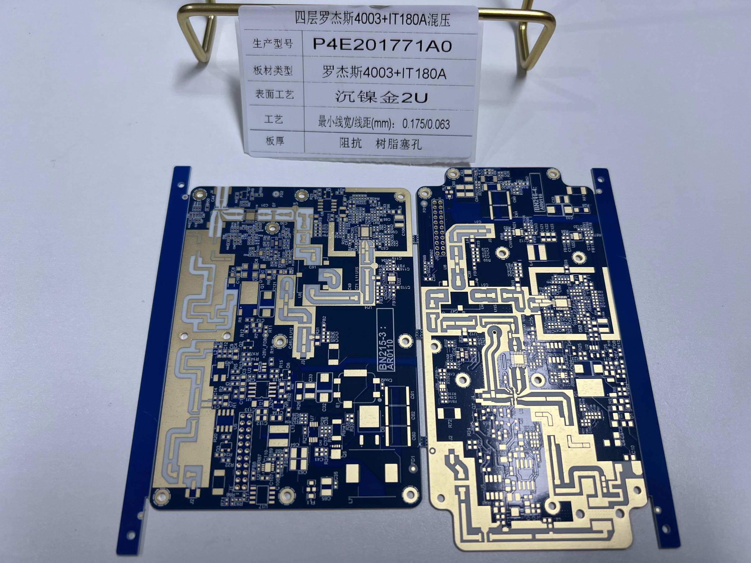
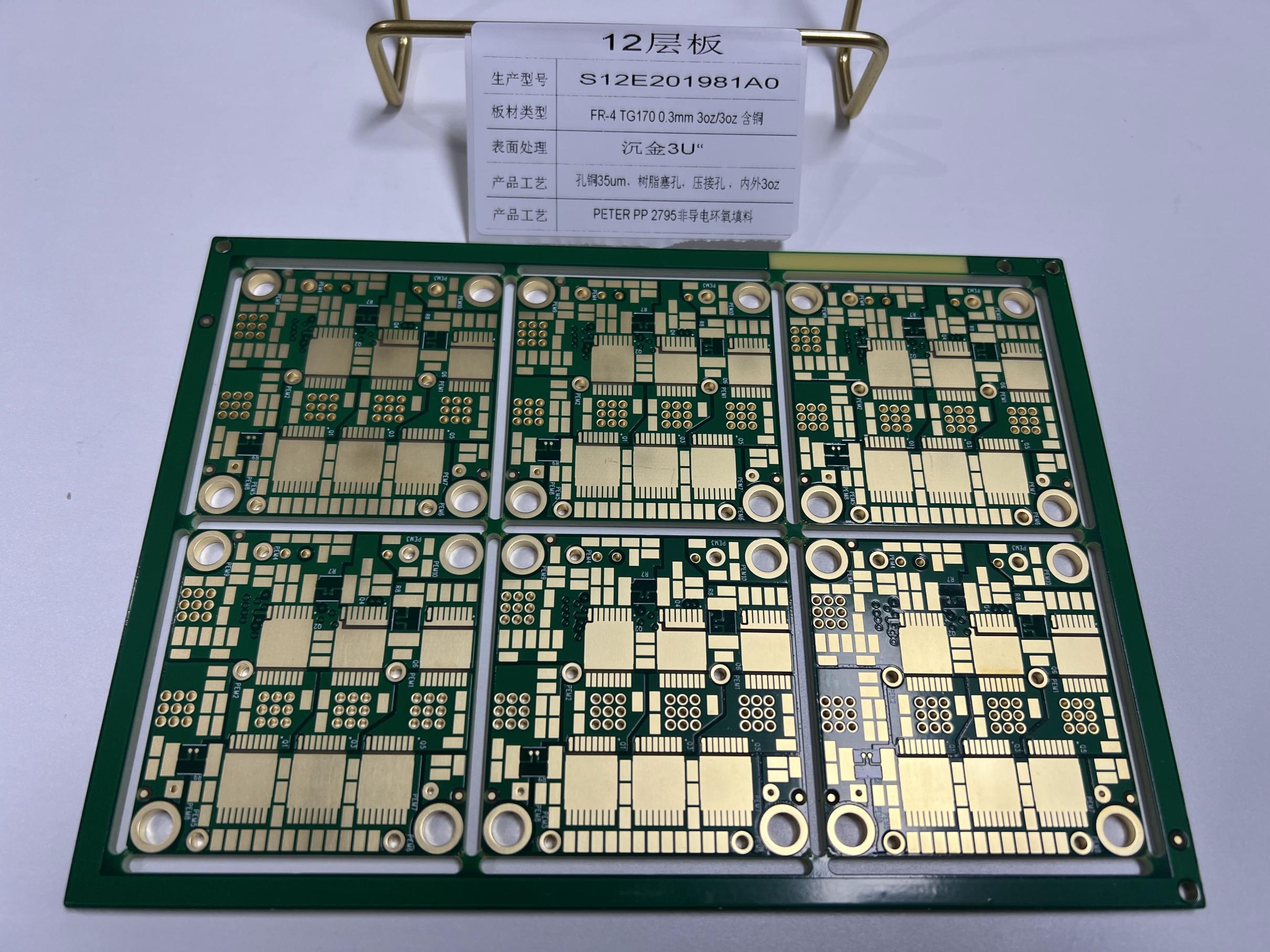
LT CIRCUIT’s skill in High-Density Interconnect lets engineers design hard boards for small devices. The company can build up to 20 layers in one PCB. This meets the needs of aerospace, medical, and automotive industries.
Two real projects show what LT CIRCUIT can do. For an autonomous vehicle, LT CIRCUIT made a 20-layer HDI PCB. It worked well in very hot and cold places and passed tough safety tests. The team used special routing and materials to help the client get speed and reliability. In another project, LT CIRCUIT made a rigid-flex PCB for a medical device. The team used 3D assembly to stack parts up and down. This made the board smaller and lighter. Careful checks and fast prototyping helped the client launch the device quickly and get good feedback.
A table below shows how LT CIRCUIT’s results compare to industry standards:
Performance Aspect | LT CIRCUIT Result / Capability | Industry Benchmark / Standard |
|---|---|---|
Intrinsic Optical Loss Rate | 26.8–82 MHz (varies by wafer treatment) | Approximately 50.8 MHz or higher |
Propagation Loss | As low as 5.6 dB/m | Around 27 dB/m |
PCB Layer Capability | Up to 12 layers | Varies, often fewer layers |
Minimum Line Width / Spacing | 3 mil / 3 mil (copper thickness 0.5 OZ) | Typically larger or less precise |
Maximum Board Thickness | Up to 8.0 mm | Varies, often thinner |
Certifications | UL, CE, ISO-9001, SGS lead-free | Industry standard certifications |
First-Pass Yield Rate (Aerospace) | 99.8% | Industry average lower |
Product Launch Speed (Medical) | 40% faster launch time | Typical launch times longer |
Defect Reduction | Up to 40% reduction via AOI, X-ray, SPC, analytics | Varies, often less effective defect control |
These results show LT CIRCUIT’s advanced processes help customers get strong, high-performance boards faster and with fewer problems.
Custom Solutions
LT CIRCUIT works closely with customers to make custom PCB solutions for many industries. The team listens to each client’s needs and gives design help, fast prototyping, and full production support. LT CIRCUIT can deliver prototypes in just 3 to 5 days. This helps customers test ideas quickly.
One example is the TINIscope system, which needed a very small and flexible PCB. LT CIRCUIT designed a rigid-flex HDI PCB with a tiny LED device (1.3 mm × 1.7 mm), a CMOS sensor with 3 μm pixels, and a half-ball lens only 2 mm wide. The team also made the optical path just 6 mm long. By removing extra chips and parts, LT CIRCUIT made the board smaller and easier to use in different places. This custom design helped the client save space and make the device more flexible.
LT CIRCUIT’s custom solutions meet the needs of many tough industries. These include telecommunications, aerospace, medical, consumer electronics, and industrial equipment. The company’s engineers use deep design talks and advanced tools to solve hard problems. Customers get boards that fit their exact needs, whether they need more layers, special shapes, or unique features.
Customers trust LT CIRCUIT because they deliver high-precision, reliable, and fast solutions for hard projects.
LT CIRCUIT’s wins include a first-pass yield rate of 99.8% for aerospace projects and a 40% faster product launch time for medical devices. The company has important certifications like UL, CE, ISO-9001, and SGS lead-free. This shows its promise to quality and safety. With strong quality control and a focus on customer needs, LT CIRCUIT stands out as a leader in custom HDI PCB solutions.
HDI Applications
Industry Use Cases
High-Density Interconnect technology is used in many fields. In cars, HDI PCBs help make smart and safe systems. They fit into small spaces in electric vehicles and driver-assistance tools. In healthcare, HDI PCBs are inside CT scanners and pacemakers. These boards move data fast and keep devices small and steady.
People use HDI PCBs in thin phones, tablets, and wearables. Some phones have boards with over 12 layers for fast memory. Communication gear, like 5G base stations, uses HDI PCBs for better signals. Aerospace and defense use these boards in satellites and radar. These places need strong and stable boards.
Reports say the HDI PCB market was $9.1 billion in 2024. It may grow to $13.9 billion by 2033. This is because people want smaller and faster devices.
Some trends are:
Microvias are getting tinier for more parts.
Any-layer interconnects give more ways to connect.
Green ways to make boards, like lead-free plating.
LT CIRCUIT Success Stories
LT CIRCUIT has helped many companies with custom HDI PCBs. The team worked with a medical company to make a tiny, bendy board for a new tool. This board made the tool lighter and easier to use. For cars, LT CIRCUIT made a 20-layer HDI PCB for a self-driving system. The board passed hard safety tests and worked in hot and cold.
A new project needed a small, tough board for a wearable. LT CIRCUIT used special materials and careful work to help. Fast prototyping and strong checks let clients launch products quickly and with fewer issues.
Project Type | Industry | Key Benefit |
|---|---|---|
Rigid-flex HDI PCB | Medical Devices | Smaller, lighter devices |
Automotive | High reliability, safety | |
Wearable PCB | Consumer Tech | Fast launch, strong build |
Customers trust LT CIRCUIT for boards that work well and help new ideas in many areas.
High-Density Interconnect technology helps make today’s electronics smaller and better.
LT CIRCUIT uses new ways to build strong and high-quality boards for tough jobs.
People who need expert HDI PCB makers can count on LT CIRCUIT for smart ideas and good results.
FAQ
What makes HDI PCBs different from standard PCBs?
HDI PCBs use microvias and fine lines. These features allow more parts to fit in a smaller space. Devices become smaller and work faster.
Tip: HDI PCBs help smartphones and medical devices stay thin and powerful.
How does LT CIRCUIT ensure quality in HDI PCB manufacturing?
LT CIRCUIT uses laser drilling, AOI, and X-ray checks. The team follows ISO standards. Each board goes through strict tests before shipping.
Can LT CIRCUIT make custom HDI PCBs for special projects?
Yes. LT CIRCUIT works with customers to design and build custom HDI PCBs. The team supports fast prototyping and full production for many industries.
See Also
How LT CIRCUIT Solves Buried Via Challenges In PCBs
LT CIRCUIT’s Expertise In Complex PCB Fabrication Services
Comprehensive Guide To Heavy Copper Multilayer PCB Production
Exploring Diverse Industry Uses For Multilayer Printed Circuit Boards
Overcoming Prototyping And Manufacturing Challenges In Multilayer PCBs