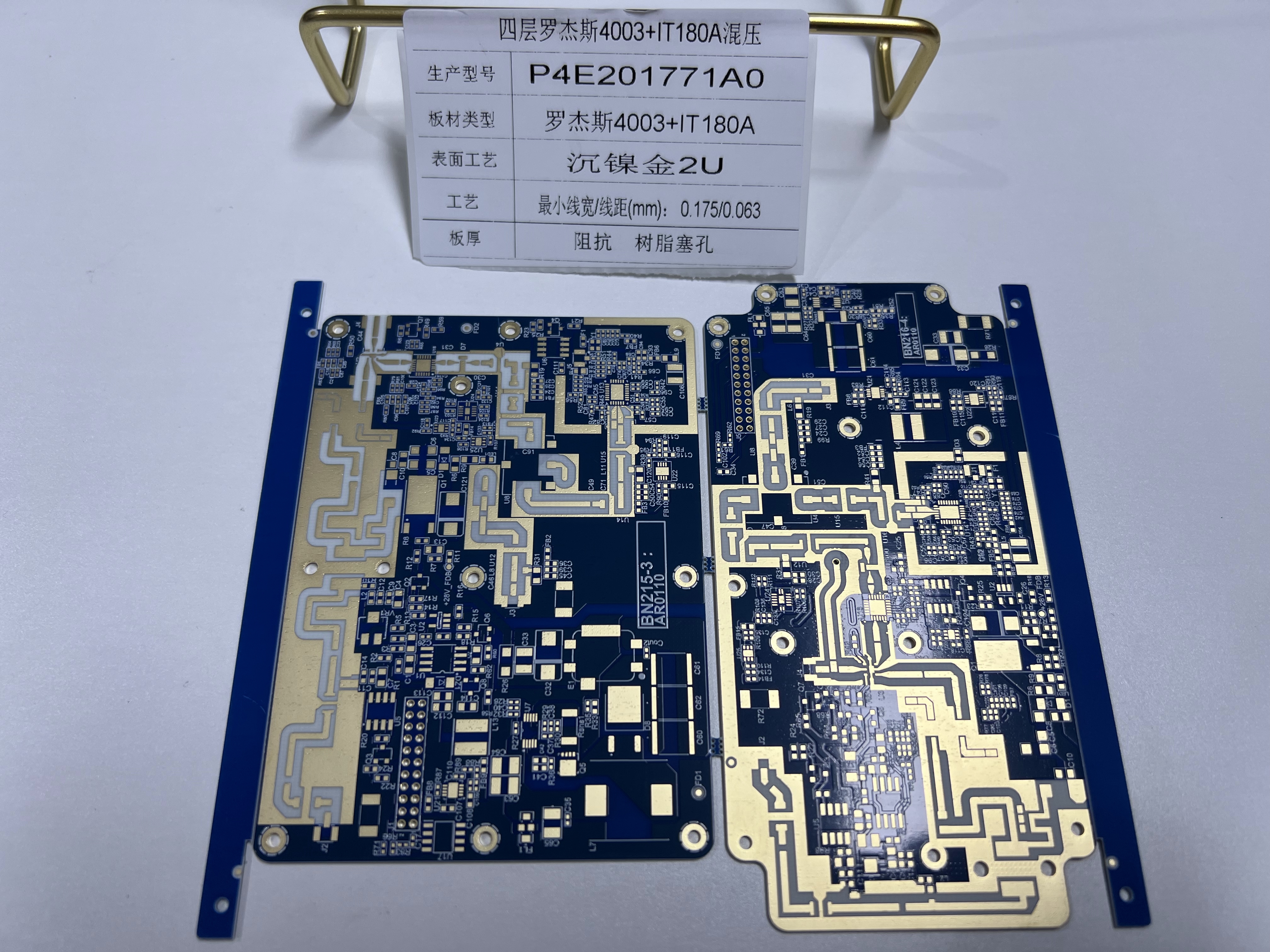
High Frequency PCBs: Manufacturing Capabilities and Design Considerations for RF Applications
High Frequency PCBs are crucial for RF applications, as they facilitate the accurate transmission of signals. Industries such as telecommunications rely on them for advancements in 5G and IoT technologies. These sectors demand faster and more reliable systems, making the design and manufacturing processes vital for maintaining signal quality. Selecting the appropriate materials and ensuring precision in production are essential factors in achieving optimal performance.
Key Takeaways
High-frequency PCBs are important for RF systems like 5G and IoT. Picking the right materials and methods helps signals stay clear.
Matching impedance is key in PCB design. Make sure traces fit the source and load to avoid signal problems or interference.
Modern methods, like laser drills and process checks, improve the strength and quality of high-frequency PCBs.
Manufacturing Capabilities for High-Frequency PCBs
Specialized Processes and Equipment for High-Frequency PCBs
Making high-frequency PCBs needs special tools and methods. These help handle the unique needs of RF systems. It's important to control impedance and block electromagnetic interference (EMI). This ensures the PCB works well. Using advanced techniques like design for manufacturability (DFM) helps improve production success. DFM helps manage impedance and lowers EMI, keeping signals clear.
High-frequency PCB production uses modern tools like laser drills and AOI systems. Laser drills make tiny holes, while AOI checks for early mistakes. X-ray inspection is also used to check inside layers and connections. This step is key to making sure RF PCBs are reliable.
Method | What It Does |
|---|---|
Improving design for production | Uses DFM to control impedance and reduce EMI for better results. |
Picking the right materials | Chooses materials with low Dk and high Tg to keep signals strong and reliable. |
Using advanced inspections | AOI and X-ray tools find problems that could hurt performance. |
Better process control | SPC tracks and adjusts production to keep quality steady. |
Material Selection for Signal Integrity and Reliability
The materials used in high-frequency PCBs affect how well they work. Low dielectric constants (Dk) and low dissipation factors (Df) are needed to avoid signal loss. Tests show that real Df values can differ from what vendors claim. For example, a Df of 0.010 at 10 GHz causes a loss of 0.95 dB/in. But a vendor's Df of 0.006 only loses 0.72 dB/in.
You also need to think about how materials handle heat and the environment. Materials with high glass transition temperatures (Tg) stay stable under heat, making them last longer in RF systems.
Tests show big differences in Df values at 1 GHz. Measured Df values are often higher than vendor claims.
For example, Df differences ranged from 33% to 200% for various materials. This greatly affects signal quality.
A measured Df of 0.010 caused a loss of 0.95 dB/in at 10 GHz. A vendor's Df of 0.006 caused only 0.72 dB/in loss. This shows a big performance gap.
Advanced Bonding Techniques and Lamination
Bonding and lamination are important for strong and reliable PCBs. New bonding methods, like SAB (Surface Activated Bonding), improve results. For example, SAB gives peel strength of 800–900 g/cm. It also keeps surface roughness below 100 nm. These improvements lower conduction loss and boost RF performance.
Improvement | Result |
|---|---|
Peel strength with SAB process | 800–900 g/cm |
Surface roughness at LCP/Cu | Less than 100 nm |
Conduction loss reduction | Three times lower than older methods |
Bonding checked by XPS analysis | Shows bulk fracture in laminate due to plasma-induced bonding sites |
Lamination also helps keep dielectric layers even. The process should avoid air pockets or uneven spots. These issues can weaken signals and make RF PCBs less reliable.
Quality Control and Testing in High-Frequency PCB Manufacturing
Quality checks are key to making good high-frequency PCBs. Manufacturers use SPC (Statistical Process Control) to watch production in real-time. This reduces mistakes and keeps quality steady. Strong monitoring methods also make production more repeatable, which is important for RF systems.
Tests like AOI and flying probe testing catch problems early. This lowers failure rates. X-ray inspection checks inside connections and layer alignment. These tests make sure the PCB meets strict RF standards.
SPC lets manufacturers track production and fix issues quickly. This reduces mistakes and improves efficiency.
Strong monitoring methods ensure steady quality and repeatable results for high-frequency PCBs.
By using advanced methods, picking the right materials, improving bonding, and doing strict quality checks, you can make RF PCBs that work well for 5G and IoT.
High-Frequency PCB Design Considerations for RF Applications
Impedance Matching and Signal Integrity
Matching impedance is very important in high-frequency PCB design. If the impedance doesn't match, signals can get distorted or noisy. This can also cause electromagnetic interference (EMI). To keep signals clear, the impedance of PCB traces must match the source and load. This stops signal reflections and reduces voltage standing wave ratio (VSWR) problems.
Using termination resistors can absorb reflected signals and keep them clear. For RF PCBs, keeping a steady 50-ohm impedance is common. This helps high-frequency signals work better and stay reliable.
Tip: Use controlled impedance traces for accurate matching. Choose materials carefully and keep dimensions precise for consistent results.
Grounding and Shielding to Minimize Crosstalk and Interference
Reducing crosstalk and interference is key in high-frequency PCB design. Good grounding and shielding can cut down noise and improve performance. A solid ground plane gives high-frequency signals a safe return path. This lowers EMI and keeps signals strong.
Shielding, like metal covers or grounded copper layers, blocks outside noise. Keeping enough space between traces also helps avoid crosstalk. These steps are crucial for RF PCBs to work well in fast communication systems.
Key Practices for Grounding and Shielding:
Use a full ground plane to keep impedance steady.
Place decoupling capacitors near power pins to reduce noise.
Add shielding cans or Faraday cages for sensitive parts.
Layout Optimization for High-Frequency PCB Design
The layout of a high-frequency PCB affects how well it works. Placing parts and routing traces carefully can reduce signal loss and noise. For RF designs, route RF traces first and keep them short and direct.
Don't run RF traces parallel to other signal traces, as this can cause interference. Use microstrip or stripline setups to control impedance. Layer stacking is also important. Putting ground planes next to signal layers lowers EMI and improves signal quality.
Note: As frequencies increase, layer alignment becomes more critical. Misaligned layers can hurt performance by causing impedance mismatches.
Trace Routing and Component Placement for RF Performance
Good trace routing and part placement are essential for RF performance. High-frequency signals need careful routing to avoid signal loss or reflections. Avoid sharp trace bends, as they can disrupt impedance. Use smooth curves or 45-degree angles instead.
For differential pairs, match trace lengths to avoid phase issues. Uneven lengths can weaken signals. Also, keep enough space between traces to reduce crosstalk and EMI.
Best Practices for Trace Routing and Component Placement:
Route RF traces first and match their impedance.
Use microstrips for short connections in shielded areas.
Keep RF traces short to reduce signal weakening.
Avoid running RF traces parallel to other signals.
Add ground planes for signal return paths.
By following these tips, your high-frequency PCB can meet RF needs. Matching impedance, grounding, good layouts, and smart routing ensure strong signals and reliable performance.
Material Considerations for High-Frequency PCBs
Dielectric Constant and Signal Propagation
The dielectric constant affects how materials handle electric fields. It controls how fast signals move and how much they weaken. Lower dielectric constants make signals travel faster, which is important for RF systems. They also reduce delays and keep signals clear.
Materials like Rogers laminates are great for high-frequency PCBs. They have low dielectric constants, which lower crosstalk between signal lines. This makes circuits more reliable. For best results, pick materials with dielectric constants between 2.2 and 3.5. Stable materials work well even with changing frequencies and temperatures. This ensures steady signals for fast communication systems.
Tip: Use materials with stable dielectric constants to keep signals strong and reduce loss.
Loss Tangent and Minimizing Signal Attenuation
The loss tangent shows how much energy turns into heat as signals move. This energy loss weakens signals and can hurt RF PCB performance. Dielectric loss, caused by the loss tangent, adds to other losses like conductor and scattering losses. Together, they decide how much signal is lost.
Materials with low loss tangents reduce dielectric loss and keep signals strong. For RF designs, lowering signal weakening is very important. Choosing materials with low dissipation factors helps circuits work well, even in tough RF conditions.
Thermal Properties and Heat Management
High-frequency PCBs create heat when they work, especially in RF systems. Materials with good heat-handling abilities and high glass transition temperatures (Tg) are important. These features stop materials from expanding too much and keep them reliable.
Pick materials that get rid of heat quickly to avoid signal problems from overheating. Good heat control also stops parts from breaking, which is crucial for RF signals.
Environmental Durability and Long-Term Reliability
Humidity and temperature changes can affect PCB materials. Long-term tests check how materials handle these challenges.
Test Type | What It Does |
|---|---|
Checks how electric fields and humidity affect materials. | |
Thermal Cycle Testing | Tests how materials handle big temperature changes over time. |
By choosing strong materials and doing careful tests, you can make sure RF PCBs stay reliable. They will handle tough environments while keeping signals clear and working well.
Common Problems and Fixes in High-Frequency PCB Design
Handling Noise and Signal Problems
Noise and signal problems can hurt high-frequency PCB performance. These issues make signals unclear, causing poor RF communication. To fix this, check insertion loss and return loss.
Term | Meaning |
|---|---|
Shows how much signal power is lost, measured in dB. | |
Return Loss (RL) | Measures power reflected back due to impedance mismatch, also in dB. |
Connection | Higher RL (above -10 dB) means lower IL, keeping signals clearer. |
To reduce interference, use good grounding and shielding methods. Add resistive feedback and reactive matching for better RF performance. Keep analog and digital traces apart to avoid crosstalk.
Controlling Heat and Keeping PCBs Stable
High-frequency PCBs can get hot during use. Too much heat can weaken signals and damage materials. Use a strong heat plan to manage this. Add thermal vias to spread heat and use aluminum or copper heat sinks to cool parts.
Other helpful ideas include:
Using fans to improve airflow.
Picking heat-resistant materials like polyimide.
Leaving enough space between parts to stop overheating.
These steps keep PCBs stable and reliable over time.
Making Sure PCBs Stay Reliable
Reliability is very important for RF systems. Heat changes and physical stress can affect how PCBs work. Tests like the Dynamic High Temperature Operating Life (DHTOL) check if PCBs can handle tough conditions.
Test Detail | What It Does |
|---|---|
Test Name | Dynamic High Temperature Operating Life (DHTOL) |
Purpose | Checks how well GaN HEMTs work under stress. |
Key Finding | Hot electron effect causes long-term damage during hard-switching. |
Running these tests helps ensure PCBs work well in hard environments.
Smart Fixes for Design and Production Problems
Fixing high-frequency PCB problems needs smart designs and advanced tools. Choose materials with good heat control and low signal loss to keep signals strong. Use simulation software to test signal paths and improve impedance.
To handle physical stress, use rounded corners and smooth trace curves. Place parts with similar sizes together to avoid stress during assembly. Add coatings to protect against water and shaking. For EMI problems, use grounding methods and ferrite beads to block noise.
By following these tips, your RF PCB will work better and last longer. It will meet the needs of modern RF systems.
Choosing LT CIRCUIT for High-Frequency PCB Manufacturing
Expertise in High-Frequency PCB Production
LT CIRCUIT is skilled in making high-frequency PCBs. They use advanced materials like Rogers RO4003C and Megtron6. These materials are great for RF systems because they work well with signals. They have low dielectric constants (Dk) and low loss factors (Df). This helps signals move faster and stay strong. For example, Rogers RO4003C has a Dk of 3.38 and a Df of 0.0027 at 10 GHz. This makes it perfect for keeping signals clear in RF designs.
Material | Type | Dk (@10GHz) | Df (@10GHz) | Tg (°C) | Td (°C) | CTE (Z, ppm/°C) | Therm. Cond. (W/m·K) | Peel Strength (N/mm) |
|---|---|---|---|---|---|---|---|---|
Rogers RO4003C | Reinforced Hydrocarbon/Ceramic | 3.38 | 0.0027 | >280 | 425 | 46 | 0.71 | 1.05 |
Rogers RO4350B | Reinforced Hydrocarbon/Ceramic | 3.48 | 0.0037 | >280 | 390 | 32 | 0.69 | 0.88 |
Megtron6 | High Frequency Material | 3.6 | 0.004 | 185 | – | 45 | – | 0.8 |
These materials also resist moisture and stay stable in tough conditions. By using these high-quality materials, LT CIRCUIT ensures your RF PCBs work well in modern systems.
Certifications and Adherence to Industry Standards
LT CIRCUIT follows strict industry rules to make reliable PCBs. They have the IPC Class 3 certification, which is the highest level for PCB quality. This means their PCBs are durable and keep signals clear for a long time.
Certification Level | Description |
|---|---|
IPC Class 3 | The highest level of certification for PCBs, ensuring strict quality and reliability requirements are met. |
When you choose LT CIRCUIT, you get PCBs that meet top standards. These are great for important uses like telecom and aerospace.
Advanced Technical Capabilities and Customer Support
LT CIRCUIT uses modern tools to make precise PCBs. They have laser drills and AOI systems to check for mistakes. These tools help create PCBs with controlled impedance and less interference.
They also offer great customer support. Their team helps with material choices and layout designs. This ensures your RF PCBs are made just right for your needs.
Proven Track Record and Customer Success Stories
LT CIRCUIT has a history of making great RF PCBs. They’ve helped industries like telecom, IoT, and aerospace. Their PCBs are used in 5G base stations and radar systems. These projects need strong signals and reliable designs.
By working with LT CIRCUIT, you get expert help and high-quality PCBs. This ensures your RF projects succeed.
Matching how PCBs are made with their design helps them work well. Picking the right materials stops signals from weakening. Good layouts keep signals clear and strong. Careful manufacturing makes PCBs last longer. LT CIRCUIT uses skill, top materials, and exact methods to meet RF needs. This makes them a trusted choice for great PCB solutions.
FAQ
What matters most when designing high-frequency PCBs?
Picking the right materials is very important. Use materials with low dielectric constants and loss tangents. This keeps signals strong and reduces weakening in RF systems.
How do you lower electromagnetic interference (EMI) in high-frequency PCBs?
Add a solid ground plane and proper shielding. Use impedance-controlled traces to block noise. These steps keep signals clear in RF designs.
Why is controlled impedance important for RF PCBs?
Controlled impedance keeps signals steady by matching source and load. It stops reflections, cuts noise, and improves how high-frequency circuits work.
See Also
Choosing PCB Materials for Effective Communication Devices
Understanding High-Speed PCB Design and Its Importance
Manufacturing Rigid PCBs: Key Materials and Quality Processes