Key Manufacturing Requirements for High-Frequency Wireless Communication PCB
High-frequency PCBs power 5G networks, IoT devices, and satellite links. The global RF PCB market reached roughly USD 8.4 billion in 2025, with Asia Pacific holding 42.8 percent of revenue. Yet your board's success depends on more than clever design. High-frequency pcb manufacturing determines whether signals stay clean or degrade. What requirements are non-negotiable for signal integrity and reliability? You must master three pillars: advanced materials, precision design, and thermal management. Each one shapes how your high-frequency wireless communication pcb performs in the field. The high-frequency pcb substrate market, valued at USD 3.22 billion in 2025, reflects this demand. Manufacturers who ignore these pillars risk failure. Those who embrace them build high-frequency pcbs that endure.
Key Takeaways
Choose PCB materials with low dielectric constant and low dissipation factor for high-frequency signals.
Maintain controlled impedance with tight tolerances to prevent signal reflection and data errors.
Use smooth copper foil to reduce insertion loss and improve signal integrity at high frequencies.
Design thermal vias and select high-conductivity substrates to manage heat and stabilize performance.
Minimize signal discontinuities by optimizing via design and component placement.
Implement effective grounding and shielding to reduce electromagnetic interference and ensure compliance.
Partner with a manufacturer that performs DFM checks to ensure producibility and reliability.
Apply these requirements to meet the demands of 5G, automotive radar, and satellite communications.
Defining High-Frequency Wireless Communication PCB
The High-Frequency Domain
Frequency Spectrum for Wireless Communication
You encounter high-frequency printed circuit boards in systems that operate above 1 GHz. Industry definitions vary somewhat. One source describes RF PCBs as covering roughly 100 MHz to several GHz, while microwave PCBs span 300 MHz to 300 GHz. Another definition places high-frequency PCBs above 1 GHz. These boards serve 5G infrastructure, radar modules, and satellite transceivers.
Why Standard FR-4 is Insufficient
Standard FR-4 laminate cannot support these frequencies. At 10 GHz, FR-4 exhibits a dielectric constant (Dk) of 4.3 and a dissipation factor (Df) of 0.020. These values cause substantial signal degradation. Mid-loss FR-4 improves Df to 0.012 and remains usable to 10 GHz. Megtron 6 drops Df to 0.004 and supports operation to 25 GHz. Rogers RO4350B achieves Df of 0.0037 and works well to 40 GHz. You must select materials that match your frequency target.
Signal Loss and Degradation
Insertion Loss and Skin Effect
The skin effect concentrates current flow near the conductor surface as frequency rises. At 10 GHz, skin depth in copper measures 0.66 μm, roughly 2 percent of 1 oz copper thickness. At 28 GHz, skin depth shrinks to 0.39 μm. Conductor loss for a 50Ω microstrip at 10 GHz reaches 0.043 dB/inch. You can calculate conductor loss using this relation: conductor loss in dB/inch = 0.433 × R_AC / Z₀, where R_AC is AC resistance per inch and Z₀ is characteristic impedance. Below 1 GHz, conductor loss dominates. Between 5 and 10 GHz, conductor and dielectric loss contribute roughly equally on standard FR-4. Above 10 GHz, dielectric loss dominates on FR-4, but conductor loss remains dominant on low-loss materials.
Impact of Impedance Mismatches
Impedance discontinuities reflect signal energy and corrupt data. You must maintain consistent trace geometry and dielectric thickness across the entire board. Every via, connector, and component pad introduces a potential mismatch. High-frequency pcb manufacturing demands tight process control to preserve impedance uniformity.
Material Selection for High-Frequency PCB Applications
Material selection for high-frequency PCB applications decides whether your design survives the field or fails on the test bench. The laminate you choose shapes every downstream step of high-frequency pcb manufacturing, from drilling to plating to final impedance verification. Standard FR-4, hydrocarbon ceramic laminate, and PTFE-based high-frequency pcb laminate materials each behave differently at gigahertz frequencies. You must weigh dielectric constant, loss tangent, and mechanical stability together.
Low Dielectric Constant (Dk)
Dk and Signal Propagation Speed
The dielectric constant, also called relative permittivity, measures how much a material stores electrical energy. Signal velocity in a high-frequency pcb falls as the square root of Dk rises. A lower Dk therefore pushes your signal faster through the trace. The propagation delay relation is tpd = sqrt(Dk_eff)/c, where Dk_eff is the effective dielectric constant and c is the speed of light. Lower Dk also cuts dielectric loss, widens traces for a target impedance, and reduces crosstalk between adjacent lines. Most RF designs target a Dk between 2.2 and 3.5. Pure PTFE laminates such as RT/duroid 5880 sit at 2.20, while ceramic-filled PTFE grades like RO3003 land between 2.94 and 3.10. Standard FR-4 class materials run from 3.40 to 3.68, and the broader non-PTFE range reaches 3.5 to 4.5.
Stable Dk Across Frequencies
Your Dk must hold steady as frequency climbs. A material with drifting Dk shifts impedance and timing across the band. Rogers RO4003C specifies 3.38 with a tolerance of plus or minus 0.05 at 10 GHz, which gives you a tight, predictable window for high-frequency pcb laminates. That stability lets you model impedance once and trust it across the operating range.
Low Dissipation Factor (Df)
Df as a Measure of Signal Energy Loss
The dissipation factor, or loss tangent, is the ratio of energy lost in the dielectric to the total energy applied. It tells you how much signal energy turns into heat as the wave travels. As frequency rises, molecular polarization cannot keep pace, so dielectric loss grows. Attenuation depends on both properties, roughly as the square root of Dk times the loss tangent, and it increases linearly with frequency. High-Df materials cause greater attenuation, weaker high-frequency amplitude, and distorted eye diagrams. For RF work, choose a Df below 0.005.
Comparing Standard vs. High-Frequency Laminate Materials
The gap between standard and high-frequency pcb materials is dramatic. Standard mid-Tg FR-4 shows a Df near 0.020 at 10 GHz, while Rogers RO4003C reaches 0.0027 and RT/duroid 5880 drops to 0.0009. Rogers RO3003, a PTFE-based grade, sits near 0.0010. Panasonic Megtron 6 measures 0.004. Always check the test frequency on the datasheet, because Df is frequency-dependent.
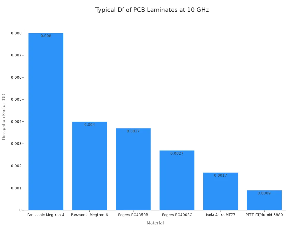
At 28 GHz the source provides no numerical Df values. It states that FR4 is practically unusable at this frequency and that PTFE-based or special low-Df ceramic-filled laminates are required for acceptable performance.
Other Material Considerations
Coefficient of Thermal Expansion (CTE) Matching
Copper conductors expand at about 17 ppm/°C. Your substrate should match that value as closely as possible. A large CTE mismatch stresses copper features during temperature cycling and can cause delamination or solder joint failure. FR4 typically shows about 11 ppm/°C in-plane and 15 ppm/°C through-plane, which illustrates the kind of range you compare against. The practical rule is simple: pick a high-frequency pcb laminate whose CTE tracks copper, rather than chasing a fixed number.
Copper Foil Surface Roughness and Its Effect on Loss
At high frequencies, current concentrates near the conductor surface. Rough foil lengthens that current path and raises insertion loss. Standard electrodeposited foil with RMS roughness of 2 to 8 μm can push insertion loss above 0.5 dB/inch at 28 GHz. Low-profile foil at Ra around 0.3 to 0.5 μm reduces skin-effect loss. Very-low-profile foil with Rz below 2 μm and Ra around 0.1 to 0.3 μm improves insertion loss by 20 to 40 percent versus standard foil above 20 GHz. Reverse-treated foil delivers 50 to 70 percent of that benefit and suits 6 to 20 GHz designs. Smoother copper also supports impedance control and limits crosstalk. Pairing smooth foil with low-Df high-frequency pcbs gives you the cleanest signal path your pcb manufacturing flow can produce.
High-Frequency PCB Manufacturing: Design and Fabrication
Impedance Control and Matching
Trace Width, Spacing, and Dielectric Thickness
You cannot treat impedance as a design-only concern. Every high-frequency pcb manufacturing step shifts it. Trace width, dielectric height, and copper thickness all move characteristic impedance. A 0.025 mm change in trace width shifts impedance by about 5–6 Ω. The same change in dielectric thickness shifts it by 5–8 Ω. Wider traces lower impedance. Thicker dielectric raises it. Lower dielectric constant also raises it.
Spacing matters just as much. Traces placed too close together raise mutual capacitance and crosstalk, which lowers effective impedance. A 0.1 mm gap can cut impedance by 5–10 percent. Keep spacing at roughly 3× the trace width. Push it to 5× for signals above 1 GHz. Differential pairs need uniform geometry to hold targets such as 100 Ω for USB and Ethernet or 90 Ω for USB 3.0.
Controlled Impedance Traces in Manufacturing
Tolerance targets separate good boards from marginal ones. Standard controlled impedance sits at ±10 percent. Critical 5G and RF designs demand ±5 percent or even ±3 percent. Dielectric thickness for critical designs holds to ±5 percent. Trace width during high-frequency pcb etching holds to ±10 percent for simulation and ±5 percent for critical work. Fabricators apply photomask compensation to correct etch undercut and pattern transfer errors.
Parameter | Manufacturing tolerance |
|---|---|
Controlled impedance | ±10% standard; ±5% or ±3% for critical 5G/RF |
Trace width (etching) | ±10% simulation; ±5% critical |
Dielectric thickness | ±5% critical; 10-mil target drift shifts impedance 2–3 Ω |
Process control | Test coupons per panel verify impedance |
Automated laser direct imaging tightens this further. Traditional photolithography shows 15–20 µm of trace width variation. LDI holds deviation below 5 µm and registers layers to ±5 µm. It supports 50/50 µm lines and spaces with a laser spot of 25 µm or less. Cleaner rectangular profiles reduce skin-effect loss. Consistent copper plating then locks impedance across the panel.
Minimizing Signal Discontinuities
Strategic Via Design and Stub Reduction
Vias create both parasitic capacitance and inductance. Together they form resonant circuits in the GHz range. Backdrilling removes excess stub material after plating and pushes stub length near zero. Blind and buried vias limit connection span. Via-in-pad smooths impedance transitions in dense routing. Ground via shielding confines return currents and cuts loop area. Antipad optimization tunes parasitic capacitance against return-path integrity. Larger diameters lower inductance, and shorter lengths reduce stub effects. Avoid unnecessary layer transitions on critical nets.
Component Placement and Routing
Placement drives parasitic behavior. A 2.54 cm trace at a high-speed op-amp input produces roughly 29 nH of stray inductance, enough to start low-level oscillation. A ground plane suppresses that inductance. Even 1 pF of parasitic capacitance at an inverting input can cause 2 dB of peaking, and more than 1 pF can trigger instability. Keep noisy and sensitive lines apart. Avoid long parallel runs. Select components with low equivalent series resistance and low equivalent series inductance. Controlled impedance routing and differential signaling dampen reflections and cut bit errors.
Grounding, Shielding, and DFM Checks
Effective Ground Planes and EMI Reduction
A continuous ground plane gives you a low-impedance return path. Gaps in that plane act as antennas, so eliminate them. Stitching vias near high-speed signals provide short return paths. Guard traces contain fields and limit coupling. Metal shielding blocks RF emissions that plastic would pass through. Place high-speed components near the board center to reduce edge emissions. Keep analog and digital circuits separate. Add bypass and decoupling capacitors at IC power pins, and use ferrite beads on power lines. Test against FCC and CE limits, which are comparable for emissions.
Role of High-Frequency PCB Manufacturer in DFM
Your high-frequency pcb manufacturer owns producibility. DFM checks confirm that material choices stay within fabrication tolerances. They verify via placement, stackup planning, and edge plating before tooling begins. Simulation plus near-field scanning and time-domain reflectometry validates the layout against targets. IPC-2221 guides board parameters that affect electromagnetic performance, and the IEC 61000 series sets EMC test limits. A partner offering one-stop high-frequency pcb manufacturing aligns material, imaging, plating, and test under one roof. That integration is what keeps a high-frequency printed circuit board predictable at volume.
Thermal Management for High-Frequency PCB
Heat and Signal Performance
Temperature Effects on Dk and Df
Temperature shifts alter dielectric properties. Dk and Df drift as temperature rises. Signal velocity changes with each shift in Dk. Loss increases with each rise in Df. Impedance moves off target. You see degraded signal integrity and added noise. Elevated temperatures also stress solder joints. Micro-cracks form in the connections. Those cracks disrupt high-frequency signal paths. Maintaining stable temperatures protects every downstream fabrication step.
Consider a high-frequency wireless communication pcb in a power amplifier stage. The device heats during operation. The substrate's Dk changes. Transmission line impedance shifts. The signal reflects at each mismatch. Data quality drops. You cannot fix this with routing alone. You need a thermal strategy.
Thermal Runaway Risks
Thermal runaway creates a dangerous feedback loop. Rising device temperature increases electrical losses. More losses generate more heat. Junction temperature climbs past safe limits. The risk escalates in high-current, high-switching-frequency applications. Higher switching frequencies raise turn-on, turn-off, gate-charging, and reverse-recovery losses. When those losses exceed cooling capability, runaway begins. Poor board design worsens the situation. Uneven current distribution creates hot spots. Parasitic inductance adds stress. Inadequate thermal pathways trap heat. Multilayer boards face an extra burden because inner layers lack airflow. Consequences include catastrophic device destruction, solder fatigue, and system downtime. A thorough pcb manufacturing review addresses these hazards from the start.
Effective Thermal Strategies
Thermal Vias and Metal Backing
Thermal vias offer one of the most effective heat paths. Place them directly under heat-generating components. Connect them to copper planes. This combination draws heat away rapidly. Junction temperature falls significantly. Metal backing provides another route for high-power designs. A metal plate spreads heat across the entire board. You reduce the temperature gradient dramatically.
High Thermal Conductivity Substrates
Substrate selection determines the board's thermal ceiling. Standard FR-4 conducts heat poorly. Its thermal conductivity sits near 0.30 W/mK. That value forces you to rely heavily on vias and copper fills. High-frequency pcb laminates with engineered fillers perform better. Materials such as Tlam SS HTD03 reach 2.2 W/mK. That substantial jump moves heat through the substrate itself.
Substrate Material | Thermal Conductivity (W/mK) |
|---|---|
Standard FR-4 | ~0.30 |
Tlam SS HTD03 (Laird Technologies) | 2.2 |
Pair a high-conductivity substrate with a low-Df core. You get both signal integrity and thermal stability. The board stays cool. The dielectric properties stay stable. The circuit holds its impedance across the operating range.
You must verify the thermal path during every stage of high-frequency pcb manufacturing. Simulate the heat flow. Identify hot spots. Add vias where needed. Choose substrates that fit your power budget. This discipline separates reliable boards from field failures.
Applications Demanding These Requirements
These requirements gain meaning in real systems. Each application blends material science, precision fabrication, and thermal control.
5G and Millimeter-Wave Systems
Ultra-Low Loss Materials
5G spans two frequency domains. Sub-6 GHz networks use hydrocarbon/ceramic laminates or hybrid FR-4 stacks. Millimeter wave pcb designs for 24–40 GHz demand high-frequency pcb materials such as PTFE, ceramic-filled PTFE, or LCP.
Dielectric targets separate the tiers. Above 5 GHz, aim for a dissipation factor below 0.005. The mmWave regime demands Df of 0.002 or lower.
Material family | Typical Dk | Typical Df | Suitable for |
|---|---|---|---|
High-performance FR-4 | 4.2–4.5 | 0.012–0.02 | Short RF traces, digital sections |
Hydrocarbon/ceramic | 3.0–3.5 | 0.002–0.004 | Sub-6 GHz, mmWave 5G |
PTFE / ceramic-filled PTFE | ~2.1–2.5 | Down to ~0.0004 | mmWave FR2, radar, satellite |
Precision for Phased Array Antennas
Phased arrays multiply the precision burden. Consistent phase across every element matters. Dk stability over temperature and humidity determines beam steering accuracy.
Lower Dk widens your 50Ω traces and loosens tolerances. High-frequency pcb laminates with stable constants let you trust the model across production lots. Laser direct imaging holds trace variation below 5 µm.
Automotive Radar and ADAS
Reliability for Safety-Critical Systems
Automotive radar operates at 77 GHz. Your high-frequency pcb applications carry functional safety weight. ISO 26262 ASIL D demands SPFM ≥99%, LFM ≥90%, and PMHF below 10 FIT.
AEC-Q200 requires 1000 temperature cycles from -40°C to +150°C and humidity bias at 85°C/85% RH. IATF 16949 mandates SPC, PPAP, and FMEA. IPC-6012 Class 3/A adds 1000+ IST cycles and 100% impedance verification. High-reliability circuit boards pass these gates.
Thermal Management in Harsh Environments
The radar module sits behind the fascia, exposed to engine heat and winter cold. Ceramic-filled PTFE materials hold Dk stable across temperature swings.
Thermal vias under the transmitter draw heat into copper planes. A metal backing plate spreads the heat. Without these, impedance drifts and object detection degrades.
Satellite and Aerospace Communication
Performance in Extreme Conditions
Spacecraft electronics face vacuum, radiation, and thermal swings. Materials must pass ASTM E595 outgassing limits. Polyimide and ceramic substrates handle these extremes.
Design for launch vibration and shock while preserving signal integrity. Controlled impedance, shielding, and conservative spacing for high-voltage nodes protect the payload.
Material Stability and Reliability
Material selection determines mission life. PTFE and ceramic-filled materials give low loss and stable phase. Low-CTE substrates between 4–7 ppm/°C reduce thermal stress against silicon devices.
Underfill protects solder joints during expansion. Thermal cycling from -55°C to +125°C validates the design. Cross-section analysis verifies plating. Every high-frequency pcb manufacturing step needs space-grade traceability.
Microwave/rf designs for satellite payloads depend on these disciplines. Microwave pcb fabrication for Ka/Q-band front-ends demands ultra-low Df. Your microwave/rf applications inherit these standards. Pcb manufacturing locks in that reliability.
Manufacturing is the bedrock of high-frequency PCB performance. You cannot separate a clean signal from the process that builds the board. Material science delivers low Dk and low Df laminates. Precision design locks impedance control across every trace. Thermal management keeps dielectric properties stable under heat. A holistic approach ties material selection to final fabrication. Future wireless technologies will demand more:
Low-loss PCB materials that minimize signal attenuation at terahertz frequencies
Higher manufacturing resolution for sub-millimeter antenna dimensions
Improved chip-to-PCB interconnect and packaging to preserve signal integrity
Your high-frequency pcb manufacturing partner must meet these rising demands. Every step in pcb manufacturing shapes whether your design survives the field.
FAQ
What frequency range defines a high-frequency PCB?
You enter the high-frequency domain above 1 GHz. Industry definitions vary. Some sources place RF PCBs from 100 MHz to several GHz. Microwave PCBs span 300 MHz to 300 GHz. Your target application determines the exact threshold. Above 1 GHz, standard FR-4 struggles with signal loss and impedance control.
Why can't I use standard FR-4 for my 10 GHz design?
Standard FR-4 shows a Dk of 4.3 and a Df of 0.020 at 10 GHz. Those values cause substantial signal degradation. Mid-loss FR-4 improves Df to 0.012 and remains usable to 10 GHz. Megtron 6 drops Df to 0.004 and supports operation to 25 GHz. You must match materials to your frequency target.
What Df value should I target for RF designs?
Aim for a dissipation factor below 0.005 for RF work. Rogers RO4003C reaches 0.0027 at 10 GHz. RT/duroid 5880 drops to 0.0009. Rogers RO3003 sits near 0.0010. Panasonic Megtron 6 measures 0.004. Always check the test frequency on the datasheet because Df changes with frequency.
How does copper foil roughness affect insertion loss?
Rough foil lengthens the current path and raises insertion loss. Standard electrodeposited foil with RMS roughness of 2 to 8 μm can push insertion loss above 0.5 dB/inch at 28 GHz. Low-profile foil at Ra around 0.3 to 0.5 μm reduces skin-effect loss. Very-low-profile foil improves insertion loss by 20 to 40 percent versus standard foil above 20 GHz.
What impedance tolerance should I specify for 5G designs?
Standard controlled impedance sits at ±10 percent. Critical 5G and RF designs demand ±5 percent or even ±3 percent. Dielectric thickness for critical designs holds to ±5 percent. Trace width during high-frequency pcb etching holds to ±10 percent for simulation and ±5 percent for critical work. Fabricators apply photomask compensation to correct etch undercut.
How do thermal vias protect signal integrity?
Thermal vias draw heat away from heat-generating components. Place them directly under those components and connect them to copper planes. Junction temperature falls significantly. Stable temperatures protect dielectric properties. Dk and Df stay predictable. Impedance holds its target. The circuit maintains signal integrity across the operating range.
What thermal conductivity do high-frequency substrates offer?
Standard FR-4 conducts heat poorly at near 0.30 W/mK. High-frequency pcb laminates with engineered fillers perform better. Materials such as Tlam SS HTD03 reach 2.2 W/mK. That substantial jump moves heat through the substrate itself. Pair a high-conductivity substrate with a low-Df core for both signal integrity and thermal stability.
Which standards govern automotive radar PCB reliability?
Automotive radar operates at 77 GHz. ISO 26262 ASIL D demands SPFM ≥99%, LFM ≥90%, and PMHF below 10 FIT. AEC-Q200 requires 1000 temperature cycles from -40°C to +150°C and humidity bias at 85°C/85% RH. IATF 16949 mandates SPC, PPAP, and FMEA. IPC-6012 Class 3/A adds 1000+ IST cycles and 100% impedance verification.
How does a high-frequency pcb manufacturer support DFM?
Your high-frequency pcb manufacturer owns producibility. DFM checks confirm material choices stay within fabrication tolerances. They verify via placement, stackup planning, and edge plating before tooling begins. Simulation plus near-field scanning and time-domain reflectometry validates the layout against targets. A partner offering one-stop high-frequency pcb manufacturing aligns material, imaging, plating, and test under one roof.
