What is High-Speed PCB Design and Why It Matters
High-speed PCB design makes circuit boards work with fast signals. It is important for modern electronics like 5G and IoT devices. This design keeps signals clear for reliable use in phones, smart cars, and data centers.
Key Takeaways
High-speed PCB design is important for today’s electronics. It keeps signals clear and steady in gadgets like phones and 5G devices.
Keeping signals strong matters. Using paired wires and avoiding sharp turns helps devices work better.
Managing EMI well with flat ground layers and good shielding lowers noise and makes PCBs work smoothly.
Key Concepts in High-Speed PCB Design
Signal Integrity in High-Speed PCB Design
Signal integrity is key for making high-speed PCBs work well. It means signals can move through circuits without losing quality. Bad signal integrity can cause errors, timing problems, and less reliable systems.
Many things affect signal integrity, like mismatched impedance, crosstalk, and signal reflections. For example:
Crosstalk happens more at high frequencies, causing nearby traces to interfere.
Copper roughness and skin effect can change signals, seen in S-parameter tests.
Jitter and inter-symbol interference (ISI) shrink signal gaps, making recovery harder.
To fix these issues, use differential pair routing. This method blocks noise and reduces the need for a return path. Avoid sharp 90-degree trace bends and keep ground planes smooth to lower interference. Tools like Ansys HFSS and Cadence Sigrity help check signal integrity and improve designs.
Metric | Why It Matters |
|---|---|
Keeps signals steady across different frequencies. | |
Noise Reduction | Stops interference that can mess up signals. |
Timing Accuracy | Helps signals stay in sync for fast systems. |
Signal Quality | Makes sure data moves reliably through the PCB. |
Focusing on signal integrity helps signals stay strong across the PCB. This leads to better system performance and reliability.
Impedance Control for High-Speed Digital Design
Impedance control is important for keeping signals clear in fast PCBs. Impedance is the resistance signals face as they move through traces. If impedance changes too much, signals can bounce back, causing errors.
To manage impedance, think about these factors:
The number of layers and impedance values for each layer.
Trace width, height, and spacing on the PCB.
The base material’s dielectric constant and insulation thickness.
Production process tolerances.
Webinars on high-speed design stress xSignal setups and layouts for good impedance control. Research shows that dissipation factor (Df) differences can hurt signal integrity. Measured Df values are often higher than vendor numbers, leading to wrong estimates of dielectric loss at high frequencies like 1 GHz.
Careful PCB planning and advanced tools can reduce impedance problems. This ensures signals move smoothly across the board.
Electromagnetic Interference (EMI) Management
Electromagnetic interference (EMI) can harm high-speed PCBs by adding noise and messing up signals. Managing EMI is vital for keeping signals and power steady.
You can lower EMI with these methods:
Use smooth ground planes to cut down interference.
Add filters, shields, and grounding to handle EMI issues.
Improve signal paths and pick materials that lose less energy.
Real-world examples show these methods work:
Industry | Example | Results |
|---|---|---|
Automotive | Electric car maker fixed EMI in chargers using filters and shields. | Passed tests, charged faster, worked better, and saved energy. |
Telecommunications | Telecom company improved signal paths for 5G base stations. | Reduced signal loss, boosted data speed, and made 5G systems more reliable. |
Consumer Electronics | Smartphone maker solved EMI issues while keeping sleek designs. | Lowered EMI, balanced looks with good performance. |
Tests like CE102 and RE102 check emissions to meet rules. These tests measure noise levels across different frequencies.
Using these strategies lowers EMI, improves signals, and boosts PCB performance.
Challenges and Solutions in High-Speed PCB Design
Crosstalk and Noise Reduction Techniques
Crosstalk happens when signals from one trace affect another. This interference can cause problems with signal quality. In fast PCB designs, stopping crosstalk is very important. Here are ways to fix it:
Add guard traces and connect both ends to the ground. This blocks interference and keeps signals clear.
Follow the 3W rule. Keep traces spaced three times their width apart. This lowers unwanted signal mixing, especially near ground planes.
Pick stripline or microstrip routing based on your design needs. Tests show guard traces work differently for 50 Ohm striplines and microstrips.
Using these tips can cut noise and improve signal strength in your PCB design.
Routing Strategies for High-Speed Signals
Routing fast signals needs careful planning to avoid problems. Issues like reflections, crosstalk, and EMI can hurt performance. These routing tips help your PCB work better:
Use controlled impedance routing to stop signal bouncing and distortion.
Space parallel traces far apart and add guard traces to lower crosstalk.
Route differential pairs close together and keep them the same length. This blocks common-mode noise and improves signal quality.
For example, reflections can happen at vias or junctions due to impedance changes. Good routing and design tools can solve these problems.
Power Distribution and Grounding Best Practices
Power integrity is as important as signal integrity in fast PCBs. A strong power and grounding setup keeps signals steady and reduces EMI issues.
Keep traces far apart—at least three times their width. This lowers crosstalk and improves power flow.
Use smooth ground planes for a clear return path for signals.
Connect ground planes across layers with many vias. This creates a strong mesh for better power stability.
Place via fences around the board edges to control EMI. Space vias based on the highest frequency to cut noise.
These steps help your PCB handle both power and signals well, making it more reliable.
Practical Design Tips for Fast PCBs
Picking Materials for Good Signals
Choosing the right materials helps signals stay strong in fast PCBs. Look for things like how fast signals travel (Dk), how much signal is lost (Df), and how well materials handle heat. Lower Dk means faster signals, and lower Df means less signal loss. Rogers 3003 works well in wet places because it doesn’t soak up water. Polyimide is tough and great for bendable designs.
Property | Why It’s Important |
|---|---|
Dielectric Constant (Dk) | Helps signals move faster; lower numbers mean less distortion. |
Loss Tangent (Df) | Reduces signal loss over distance; lower numbers are better. |
Thermal Stability | Keeps performance steady when temperatures change; High-Tg materials are best. |
Moisture Absorption | Stops water from messing up signals; Rogers 3003 is a good choice. |
Mechanical Strength | Strong materials handle stress; Polyimide works well for flexible boards. |
Picking materials with these features makes your PCB work better in different situations.
Planning PCB Layers for Fast Signals
Good layer planning is key for fast PCB designs. Put signal layers near ground planes to cut interference and keep impedance steady. Symmetrical layers help balance performance and lower noise. Use materials with steady dielectric properties for better signal paths.
Tips for layer planning:
Keep signal layers close to ground planes for clear paths.
Use impedance control to stop signal problems.
Shorten trace lengths to avoid delays and noise.
Separate analog and digital signals with ground planes to reduce interference.
More layers often make routing easier and improve signal quality.
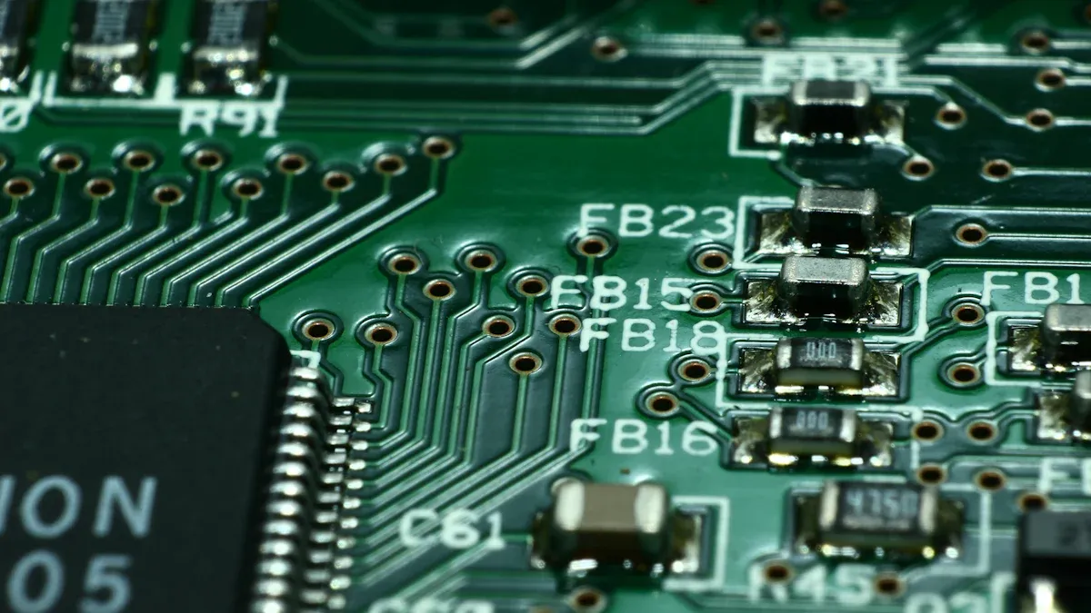
Better Via Placement for Strong Signals
Placing vias smartly improves signals and lowers noise. Short vias help signals flow better by cutting resistance. Via stitching links ground planes, making signals more stable. Putting vias under pads stops impedance problems and keeps performance steady.
Ways to improve via placement:
Use via stitching to connect ground planes and cut noise.
Place vias under pads to boost signal strength.
Keep vias short for better heat handling and signal flow.
Test via placement with design tools to find problems early.
These steps make your PCB stronger and improve signal and power flow.
Tools and Techniques for High-Speed PCB Design by LT Circuit
Simulation and Analysis Software for Signal Integrity
Simulation tools help check how fast signals work on PCBs. These tools let you see and fix problems before making the board. Issues like signal bouncing, crosstalk, and timing errors can be spotted early.
Using these tools often improves signal quality a lot. For example:
Improvement Type | Performance Gain | Scenario |
|---|---|---|
Eye Margin | General | |
PAM4 | 3x-5x | Specific |
These results show how simulations make high-speed systems more reliable. Fixing problems early ensures your PCB works well for modern devices.
Design Rule Checking (DRC) Tools for High-Speed Digital Design
DRC tools check if your PCB design follows the rules. They look for mistakes like wrong trace spacing or bad via placement. These tools also check if impedance control is correct.
Using DRC tools stops expensive mistakes during production. They also check grounding and power setups to keep your PCB stable. This makes sure your high-speed design is dependable.
Prototyping and Testing Methods for High-Speed PCB
Prototyping helps test ideas and find mistakes early. Low-cost prototypes let you check if the design works before full production. Quick prototypes save time and money by speeding up changes.
Testing methods ensure your PCB is high quality during production. Advanced tests handle complex designs and improve reliability. Early testing confirms the PCB works while other parts of the product are developed. This helps launch products faster.
High-speed PCB design helps electronics work well and efficiently. To improve performance, focus on signal quality, impedance control, and reducing interference. LT Circuit provides smart solutions to meet your needs and keep you ahead in technology.
Learning new skills is key to success. Think about these points:
Happy customers mean better service.
Keeping customers can raise profits by 25%.
Quick replies bring more repeat orders.
Handling challenges makes PCB designs better and builds your reputation.
FAQ
What is the main goal of high-speed PCB design?
The goal is to send signals quickly and reliably. It also reduces noise, interference, and signal loss in modern devices.
How does impedance control improve PCB performance?
Impedance control keeps signals steady and smooth. This lowers bouncing and distortion, making circuits more reliable.
Why is material selection important in high-speed PCB design?
Materials with low Dk and Df keep signals strong. They help data move faster and work better.
💡 Tip: Talk to experts like LT Circuit for the best PCB design results.
See Also
Explore Cutting-Edge HDI PCB Prototyping Methods Right Now
Three Major Advantages of VIPPO for PCB Development
Frequent Issues and Fixes in PCB Design for SMT Needs
Ways Fast Turnaround HDI PCBs Reduce Project Expenses by 2025
Crucial Advice for Creating Heavy Copper PCBs for High Currents