Improving High-Speed PCB Reliability with Advanced Impedance Strategies
Advanced impedance strategies help your high-speed pcb work well. Impedance control keeps your signal safe from problems. It also helps your pcb follow strict rules for data quality. You can see this in many high-speed uses:
DDR memory needs exact impedance to stop reflections and data mistakes.
Ethernet uses 100 ohms for differential pairs to lower crosstalk and EMI. These can cause packet loss.
USB needs 90 ohms for differential signaling. This keeps your data fast and safe from errors.
When you use the right impedance strategies, your circuits stay stable and work well.
Key Takeaways
Impedance control is very important for high-speed PCBs. It stops signals from bouncing and stops data mistakes. This makes sure the board works well.
Always make the impedance of traces, sources, and loads the same. This helps signals move easily and not bounce back.
Use simulation tools to check impedance before you finish your PCB design. This step finds problems early and saves time.
Keep a solid ground plane in your design. It gives a low-impedance path for signals to return. This lowers noise and keeps signals clear.
Follow industry rules for impedance tolerance. This makes sure your high-speed boards work well and meet needs.
High-Speed PCB Impedance Control
What Is Impedance Control
Impedance control means you keep the impedance of your pcb traces in a certain range. In high-speed pcb designs, traces act like transmission lines. These lines have resistance, inductance, and capacitance. You need to match the impedance of the source, trace, and load. This matching helps signals move without bouncing or losing strength. You do this by designing the trace width, spacing to the ground plane, and choosing the right materials. Impedance control makes sure high-speed signals travel smoothly from one part to another.
Why It Matters for High-Speed Signals
High-speed signals move quickly and can change direction fast. If impedance does not match, part of the signal bounces back. This bounce can change the signal and cause mistakes. You might see ringing or odd shapes in your signal. These problems can cause data loss or errors. In high-speed pcb work, you want every signal to reach its spot without delay or change. Impedance control helps you do this. For DDR memory, you keep impedance steady to stop read and write errors. Ethernet uses 100-ohm differential pairs to stop crosstalk and keep data safe. USB uses 90-ohm differential pairs for the same reason. When you control impedance, you protect signal integrity and keep your high-speed pcb reliable.
Tip: Always check the impedance needs for your application before you start your pcb design. This step saves time and stops costly mistakes.
Signal Integrity and EMI Reduction
Signal integrity means your signal stays strong and clear as it moves through the pcb. Impedance mismatches can cause many problems. Here is a table that shows what happens if you do not control impedance:
Consequence | Description |
|---|---|
Signal Reflection | Mismatched impedance makes part of the signal bounce back, causing errors. |
Signal Loss | Too much attenuation weakens the signal over distance. |
Crosstalk | EMI causes interference between signals, leading to data corruption. |
Timing Issues | Signals may arrive at different times, causing sync problems. |
Data Corruption | Signal integrity is lost, causing transmission errors. |
You can see poor impedance control leads to many issues. Reflected signals can also make electromagnetic interference (EMI). EMI can affect other parts of your pcb or other devices. Controlled impedance reduces EMI and keeps signals clean. This step is important for meeting industry standards and passing EMC tests. In real life, engineers fixed problems in DDR memory, USB 3.0, and automotive Ethernet by improving impedance control. They saw fewer errors, better signal transmission, and more reliable high-speed pcb performance.
Design Factors Affecting Impedance
Trace Geometry
You change the impedance by adjusting trace geometry. Trace width and spacing are important in high-speed pcb designs. Wider traces make impedance lower. Narrower traces make impedance higher. The space between traces and the ground plane also affects impedance. If you pick the wrong width or spacing, your transmission lines will not match the needed impedance. This can cause signal reflections and loss. For high-speed digital circuit layouts, always check the trace width and spacing for your target impedance. Use a calculator or simulation tool to find the right values.
Tip: Keep trace width and spacing the same along the whole transmission path to keep controlled impedance.
Layer Stack-Up
How you arrange layers in your pcb design changes impedance control. High-speed signal layers should be next to solid reference planes. This keeps the return path short and stable. If you change layer spacing or use different materials, impedance can shift. A common stack-up is signal-ground-power-ground-signal. This helps shield signals and manage heat. Plan your stack-up early and stick to it for reliable impedance.
Layer Arrangement | Effect on Impedance |
|---|---|
Signal next to ground | Stable, controlled impedance |
Split reference planes | Impedance jumps, more noise |
Dielectric Materials
The material between pcb layers is called the dielectric. It changes impedance. Materials like FR-4 and Rogers RO4350B have different dielectric constants. A higher dielectric constant makes impedance lower. A lower dielectric constant makes impedance higher. Dielectric loss matters too. Lower loss means better signal transmission and less signal loss at high-speed. For high-speed pcb performance, pick materials with stable dielectric properties.
Higher dielectric constant = lower impedance
Lower dielectric constant = higher impedance
Lower dielectric loss = better signal integrity
Ground Plane Importance
A solid ground plane is important for impedance control. It gives signals a low-impedance return path and keeps loop inductance low. If you break the ground plane, impedance can jump and noise can go up. Solid planes keep return currents close to the signal trace. This helps keep controlled impedance and reduces EMI.
Note: Never route high-speed transmission lines over split or missing ground planes.
Differential Pair Spacing
When you use differential pairs for high-speed transmission, spacing matters. If pairs are too close, parasitic capacitance and crosstalk go up. This can change the differential impedance and hurt signal integrity. For USB or Ethernet, keep the spacing even and follow the recommended values for your application. This step makes sure signal transmission is reliable and keeps impedance steady.
Tip: Use your pcb design rules to set and lock the right spacing for differential pairs.
Advanced Impedance Techniques
Simulation Tools
Simulation tools help you control impedance in high-speed pcb designs. These tools let you make models of transmission lines. You can see what the impedance will be before building your pcb. Here is a table with some popular simulation tools and what they do:
Tool Name | Features | Applications |
|---|---|---|
Altium | Layer stack manager for dielectric constants and trace dimensions. | Signal integrity checks for 50-ohm lines. |
Cadence Allegro | Advanced SI tools, pre- and post-layout analysis, integration with Sigrity. | Detects crosstalk and jitter in complex designs. |
ANSYS SIwave | Electromagnetic simulation, 3D field analysis, precise impedance matching. | RF and microwave circuit designs. |
HyperLynx | Robust SI simulation, user-friendly interface, batch simulations. | High-speed digital designs. |
These tools let you check your layout and signal integrity before making your pcb. You can find problems early and fix them to get better results.
Controlled Routing
Controlled routing helps you meet impedance needs in high-speed circuits. You change trace widths and other settings as you route signals. The software figures out the right trace width for your impedance. When you move to another layer, it changes the width to keep impedance steady. Reference planes give signals a good ground. This keeps impedance the same and helps signals move well. Controlled routing makes sure your lines match the design.
Tip: Always route high-speed signals over a solid ground plane to keep impedance controlled.
Impedance Calculation
You need good ways to figure out impedance in tricky pcb layouts. Here is a table with common methods:
Method/Tool | Description |
|---|---|
Wadell’s Impedance Equations | More accurate for determining pcb impedance with less than 1% error. |
Pre-Layout Simulation | Analyzes impedance before finalizing layout, allowing for adjustments to design parameters. |
Post-Layout Verification | Confirms that the actual design matches intended impedance, accounting for real-world factors. |
Differential Pair Impedance Control | Ensures precise impedance matching for high-speed designs, typically 90 or 100 ohms. |
Time-Domain Reflectometry (TDR) | Measures impedance discontinuities along a trace, identifying mismatches through reflected signals. |
You can use tools like Altium Designer, Cadence Allegro PCB Designer, and ANSYS SIwave for impedance work. These tools help you keep impedance close to your target.
High-Speed PCB Design Guidelines
High-speed pcb design starts when signals go above 50 MHz or change in less than 2 nanoseconds. You must control impedance, stop digital noise, and watch for skin effect. If your trace is longer than λm/12, you need special layout rules. Here are some best practices:
Keep a ground plane with no breaks.
Use via stitching along ground edges for low-impedance return paths.
Match delay in differential pairs.
Keep spacing of 1.5 to 2 times the trace width between high-speed traces and ground pours.
Connect ground pours to the main ground.
These steps help you control impedance and keep signals strong in high-speed digital circuits.
Impedance Verification & Challenges
Measurement Methods
You need to check impedance in your high-speed pcb. This makes sure signals move well and do not get messed up. Time Domain Reflectometry (TDR) is the main way to measure impedance. TDR sends a quick pulse down the transmission line. It looks for reflections when impedance changes. You use a pulse generator and a sampling oscilloscope for this test. Many pcb designs have measurement coupons. These coupons help you check impedance before making lots of boards. TDR gives you exact measurements without hurting the traces. It helps you find mismatches and keep impedance steady in high-speed circuits.
TDR checks impedance by sending pulses and looking at reflections.
Measurement coupons help you check transmission line impedance.
TDR gives good results for high-speed pcb samples.
Common Pitfalls
You can run into problems when checking impedance. Material properties like dielectric constant can change and affect impedance. Making the pcb, like etching, can cause small errors, especially with thin traces. Weather, like heat and wetness, can also change impedance over time. Matching impedance is very important in high-frequency designs. Sometimes, it is hard to see impedance changes on some nets during layout. These problems can mess up signals and cause errors.
Changes in material properties change impedance.
Etching mistakes can hurt thin traces.
Heat and wetness can change impedance.
Matching impedance is needed for high-speed designs.
Impedance changes can be missed during layout.
Solutions for Reliable Design
You can fix impedance problems by using good design steps for high-speed pcb. Make a stackup that keeps impedance right and has a solid ground plane under traces. Use resistors at the end of lines to match impedance. Cut down on bumps by using back-drilling for fast signals and picking the right connectors. Always test and measure impedance with TDR after making the board. This helps you find and fix mismatches. Industry rules tell you how close impedance should be for each use.
Application Type | Tolerance Level | Description |
|---|---|---|
Consumer Electronics | ±10% | Focuses on saving money with medium signal speeds. |
Industrial Control Systems | ±8% | Needs better reliability in busy places. |
5G Base Stations and Medical Equipment | ±5% | Very important for safety and good signals. |
Millimeter-Wave Radar and High-End Servers | ±3% | Needed for no mistakes at very high speeds (≥56Gbps). |
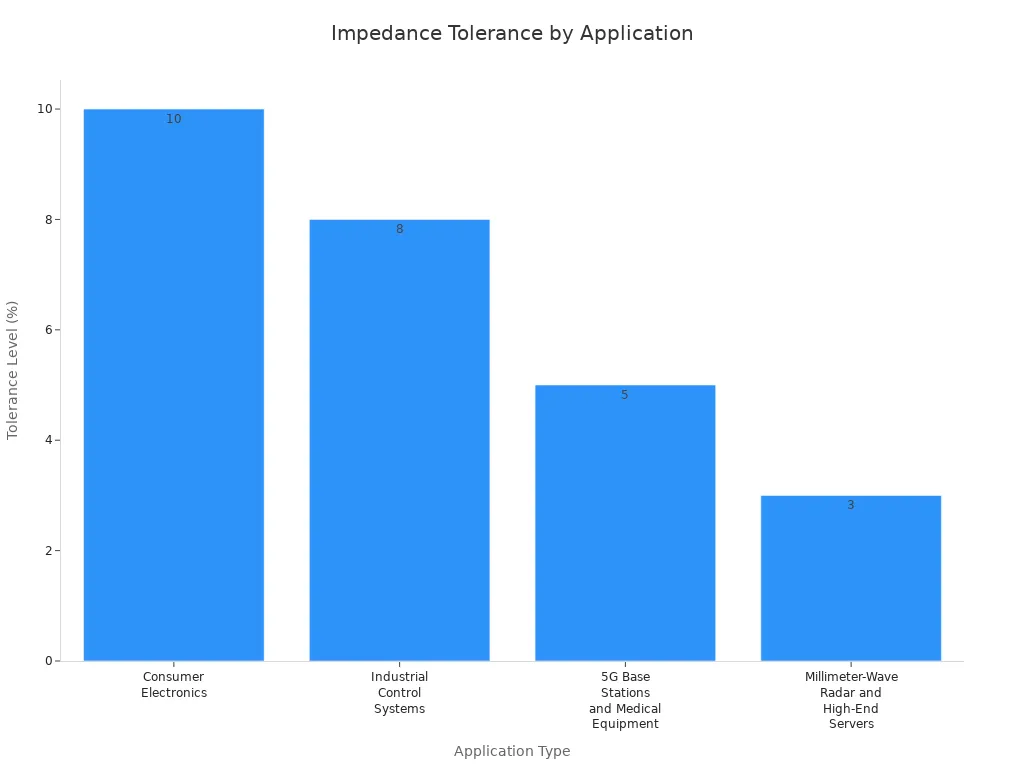
Tip: Always follow IPC rules and use TDR to check impedance. These steps help you reach your goals and keep signals working well.
You help make your high-speed PCB work well. Using advanced impedance strategies stops signals from bouncing and keeps data safe.
High-frequency applications need controlled impedance to keep signals clear and avoid data loss. If you do not control impedance, signals can bounce and get distorted. This can hurt how your circuit works and make it less reliable.
Try these steps for good results:
Use simulations and check your design.
Set clear limits for your work.
Look over fabrication notes.
Measure and watch impedance.
Keep learning about industry standards. Make impedance control a top priority to keep your circuits strong and trustworthy.
FAQ
What is controlled impedance in PCB design?
Controlled impedance means you pick the right trace width and spacing. You also choose good materials. This helps signals move with the correct resistance. Signals stay strong and do not get messed up. You use controlled impedance for fast data lines like USB, DDR, and Ethernet.
How do you measure PCB trace impedance?
You use a tool called Time Domain Reflectometer (TDR). It sends a quick pulse down the trace. The tool checks if any signal bounces back. This test finds impedance mismatches before you finish your board.
Why do differential pairs need matched impedance?
Differential pairs carry two signals that work together. If you match their impedance, both signals stay balanced. This lowers noise and keeps your data safe. USB and Ethernet designs use matched impedance for differential pairs.
What happens if you ignore impedance control?
If you skip impedance control, signals can bounce or get weak. You might see data errors or timing problems. Sometimes, your device may stop working. Always check impedance for high-speed circuits.
See Also
Enhancing Signal Integrity Through Impedance Control Techniques
Essential Design Factors for Reliable HDI PCB Production
Evaluating Costs and Benefits of Advanced HDI PCB Solutions
Top Material Choices for Designing High-Speed PCBs
Essential Steps for Implementing Multi-Impedance Control in PCBs