How Printed Circuit Boards Power the Core Functions of IoT Devices

Printed circuit boards serve as the central hardware platform that integrates and connects every critical component inside IoT devices. These circuit boards do far more than hold parts in place. They manage power delivery, keep signals clear, and enable wireless connections that define modern IoT functionality. Consider your smart thermostat. A printed circuit board inside coordinates temperature sensors, Wi-Fi chips, and display drivers simultaneously. The same principle applies across the internet of things. You will discover how PCBs enable connectivity, sensor integration, power management, and data processing. Understanding these core functions of IoT devices reveals why thoughtful PCB design determines whether your connected product performs reliably or fails in the field.
Key Takeaways
PCBs integrate and connect all critical components in IoT devices.
IoT PCBs manage power, signals, and wireless connections efficiently.
Careful PCB design ensures reliable performance in the field.
PCBs support various wireless protocols like Wi-Fi and Bluetooth.
Proper sensor placement on PCBs improves measurement accuracy.
Power management on PCBs extends battery life and stability.
PCBs enable data processing and edge-to-cloud communication.
Miniaturization and rugged materials make IoT PCBs durable.
What Is an IoT PCB
An IoT PCB is a specialized printed circuit board that serves as the hardware backbone for connected devices. Manufacturers build IoT devices on these boards, which support and connect every essential component. The PCB in IoT equipment manages power delivery, keeps signals clear, and enables wireless connections. You will find this technology inside smart thermostats, fitness trackers, and industrial sensors alike.
Structure and Materials
Conductive Layers and Substrates
A printed circuit board uses conductive copper layers separated by insulating dielectric material. The substrate provides the physical foundation, while patterned copper traces carry electrical signals between components. Inner power and ground planes distribute voltage across the board. This layered construction allows dense component placement without short circuits.
The dielectric material also affects signal speed and integrity. You should select substrates with stable electrical properties for high-frequency IoT applications. Material choice directly impacts how well your device performs in the field.
Surface Finish and Mounting
Surface finish protects exposed copper from oxidation and enables reliable soldering. Common finishes include gold, silver, and tin. Each option offers different durability and cost tradeoffs. Solder pads and plated vias create electrical and mechanical connections between components and between layers. This turns a bare PCB into a functional assembly ready for IoT PCB assembly.
The Hardware Backbone
Mechanical Support and Routing
The PCB laminate acts as a rigid structural base for mounting processors, memory, sensors, and power electronics. Placing resistors, capacitors, and ICs inside dielectric layers reduces exposed assembly mass and improves resistance to vibration and thermal cycling. Embedded components near active circuitry shorten trace lengths and lower loop inductance. This helps maintain signal integrity in constrained spaces.
Microvias and fine-line routing move signals through inner layers. Via-in-pad creates flat, plated solderable pads that directly connect fine-pitch BGAs, SoCs, PMICs, memory, and sensor hubs. These techniques free outer-layer space for antennas, sensors, and test pads.
Enabling Compact Form Factors
Thin boards measuring 0.6 to 1.0 mm, flexible structures, and reduced stack height help PCBs fit curved or folded enclosures. This enables environmental monitors and wearables to meet size limits while keeping reliable wireless connectivity. A well-designed PCB for IoT devices balances density with manufacturability.
How IoT PCBs Differ
Size, Power, and Connectivity
IoT circuit boards must fit analog sensors, digital processing, power management, and RF transceivers into a severely constrained footprint. Every microamp of leakage current compounds, so components must be chosen carefully. RF transceivers must integrate with sensitive analog and noisy digital circuits. A flawed matching network lowers antenna efficiency, forces retransmissions, and drains battery.
Dimension | Conventional PCB | IoT PCB |
|---|---|---|
Size | Forgiving spatial margins | Severely constrained footprint |
Power | Standard regulators acceptable | Every microamp matters |
Wireless | RF layout not critical | RF integration essential |
Environmental and Reliability Demands
IoT PCBs face moisture, vibration, and temperature extremes. You need conformal coating and rugged materials for outdoor or industrial deployments. Reliability demands exceed those of consumer electronics. These requirements shape every decision in IoT PCB design.
The Role of Printed Circuit Boards in IoT Devices
You are exploring the role of printed circuit boards in IoT devices by following the path signals and power take inside a smart product. A printed circuit board sits at the center of every smart product. It acts like a roadmap for electricity, guiding every voltage level and data pulse to the correct destination. This roadmap simplifies how sensors, processors, and radios link together. Without it, a smart thermostat could not coordinate its temperature sensor, Wi-Fi chip, and display driver.
Connectivity and Signal Flow
Connectivity depends on how clearly the board carries high-frequency signals. Every trace, via, and plane changes the signal path. A well-designed board keeps those paths stable.
Routing Wireless Signals
The PCB routes wireless signals between the antenna and the radio module. IoT PCB designers place antennas near the board edge, away from metal. Impedance-controlled traces hold signals on a stable path, reducing degradation for Wi-Fi and Bluetooth. A ground plane underneath the antenna trace blocks unwanted noise. Minimize trace length to reduce signal loss. Use thick signal traces to lower high-frequency losses.
Managing Interference and Loss
Signal loss and interference threaten every wireless link. Careful IoT PCB design controls these problems. Keep high-speed traces short and direct. Maintain consistent trace width to avoid impedance mismatches. Avoid long parallel traces, because crosstalk corrupts data. Reduce dielectric height to minimize crosstalk. Space signal groups three trace widths apart. Choose dielectrics with a consistent constant for high-frequency operations. Terminate signals with the correct impedance value to prevent reflections. Use multilayer boards with dedicated ground planes. Place decoupling capacitors near power pins. Shielding techniques, such as copper pours and guard traces, protect sensitive circuits from electromagnetic interference.
Supporting Communication Protocols
PCBs in IoT devices must support many communication standards. Module selection and board layout decide which protocols work.
PCB function | What the PCB does |
|---|---|
Power distribution | Moves the right voltage to sensors, chips, and radios. Smart power paths and low-power components save energy. |
Signal integrity | Creates electrical roadways that link microcontrollers, sensors, and wireless modules. Controlled impedance keeps signals strong. |
Wireless connectivity | Hosts antennas and RF modules while meeting regulatory and safety rules in a compact design. |
Wireless Protocol Support
Wi-Fi, Bluetooth, Zigbee, LoRa, and cellular each place different demands on the board. A PCB for IoT devices integrates antenna and RF modules that match these protocols. Some PCBs include multi-protocol modules that support firmware updates and future wireless technologies. Compact form factors, efficient power management, and integrated antennas belong in the design. IoT systems also adopt NB-IoT and Sigfox for low-power wide-area networks.
Wired Interface Support
Not every connection uses radio waves. Smart devices often use wired interfaces such as Ethernet, USB, and I2C. The PCB routes these signals without crossing sensitive analog or RF paths. Proper spacing and termination prevent reflections. Wired links remain essential in industrial gateways and diagnostic ports.
Enabling Device-to-Device Communication
Reliable device-to-device communication depends on disciplined layout. PCBs in IoT use precise trace design, grounding, and shielding to send clean data between nodes.
Trace Design for High-Speed Data
High-speed data buses demand careful PCB layout. Keep differential pairs close and equal in length. Minimize vias on critical paths because vias create impedance discontinuities. Use controlled impedance traces for high-speed buses. Avoid crossing split planes. If you must cross, add stitching capacitors. Route the clock to the longest delay path so data settles before the clock reads it. Wide power traces reduce resistance and waste.
Grounding and Shielding
Dedicated ground planes stabilize signals and prevent ground loops. A continuous ground plane beneath signal layers minimizes noise. Place ground planes under antenna traces to block noise. Shielding layers or metal enclosures protect sensitive components. Differential signaling lowers electromagnetic interference. Multilayer stack-ups that separate power, ground, and signal improve range. A multilayer PCB isolates these layers for cleaner communication. Simulate RF behavior before prototyping to identify interference early. Use stitching capacitors when a trace must cross a split plane.
Every design decision on an IoT circuit board determines whether your product communicates reliably. IoT circuit boards continue to shrink yet carry more protocols each generation. A complete PCBA includes microcontrollers, memory, and wireless modules. This IoT PCBA turns the bare board into a working device.
Sensor and Module Integration
Sensors act as the sensory organs of an IoT PCBA. They detect temperature, humidity, motion, and light, then convert these physical quantities into electrical signals. Communication modules let your IoT devices exchange data with other devices or the internet. You will find Wi-Fi, Bluetooth, Zigbee, LoRa, and cellular modules mounted alongside these sensors on most circuit boards.
Mounting Sensors on PCBs
Surface Mount and Through-Hole
Surface mount technology dominates modern IoT PCB assembly. Small sensors sit directly on solder pads, which saves space and supports automated production. Through-hole mounting remains useful for larger components that need extra mechanical strength. You should choose the method that matches your sensor package and your production volume.
Placement for Accuracy
Sensor placement determines measurement accuracy. Keep temperature sensors away from power regulators and processors that generate heat. Place motion sensors at the board edge so enclosure walls do not block their field of view. Route analog signal traces away from high-speed digital lines to prevent noise from corrupting readings.
Connecting Modules and Peripherals
Common Interface Standards
Your PCB connects modules through several serial protocols. Each protocol offers distinct tradeoffs.
Protocol | Wires | Typical Speed | Key Feature / Use Case |
|---|---|---|---|
UART | 2 | ~1 Mbps | Debugging, GPS modules, simple point-to-point communication |
I2C | 2 | ~400 kHz | Multiple devices on a shared bus; sensors, RTCs, EEPROMs |
SPI | 4 | 10+ Mbps | Faster, full-duplex; displays, flash memory, SD cards |
Use UART for simple point-to-point links, I2C when you want many low-speed sensors on two wires, SPI when you need speed and don't mind extra wires, and CAN when you need robust, multi-node communication in noisy industrial or automotive environments.
Most modern microcontrollers expose multiple independent peripheral blocks. A UART link, an I2C bus, and an SPI bus can all run simultaneously on one MCU.
Power and Data Lines
Every module needs both power and data connections. Dedicate separate traces for voltage and ground to each peripheral. Add decoupling capacitors near module power pins to smooth voltage fluctuations. Keep data lines short and matched in length when timing matters.
Supporting Modular Designs
Daughterboards and Shields
Modular PCB design splits your system into functional boards that you can develop, verify, replace, and reuse. A daughterboard is one physical module type within this architecture. Stacked boards, backplanes, and cable-linked assemblies also support modularity. Choose the architecture based on your service model, signal bandwidth, and upgrade path.
Interchangeable Components
Interchangeable components let you diagnose and replace failed or outdated functions independently. This approach works when connectors remain accessible and you document safe replacement procedures. Modularity can reduce redesign and service cost, though it may increase unit hardware cost. A monolithic board may be preferable when your product is small, cost-sensitive, and built in one stable configuration.
Power Management on IoT PCBs
A stable power source determines whether your IoT device operates reliably or fails unpredictably. The power supply on a PCB ensures every component receives the correct voltage and current. Battery management systems and voltage regulation form the foundation of this stability. You must design power delivery carefully to meet the demanding requirements of connected devices.
Distributing Power to Components
Power Planes and Traces
Power and ground planes provide low-impedance paths for return currents. These structures reduce noise and electromagnetic interference while improving power delivery during sudden current spikes. Trace routing, including width, thickness, and length, strongly affects resistance and voltage drop. You should optimize trace width and copper thickness to lower resistance and improve current-carrying capacity. Undersized vias in high-current paths introduce significant voltage drops. Place components closer to the ground plane and use multiple power planes with stitching capacitors to reduce voltage fluctuations.
Voltage Regulation
Voltage regulators maintain stable output despite battery voltage changes. High-efficiency low-dropout regulators cut power losses compared with traditional linear regulators. Efficient DC-DC converters step down battery voltages to logic levels with minimal losses. Buck converters suit intermittent sensor duties. Keep DC-DC power output traces short and wide so they carry the required current. Place feedback components close to the IC pins and route feedback traces away from high-current power planes.
Enabling Low-Power Operation
Sleep Modes and Power Gating
Many microcontrollers support deep sleep or standby states where the core is off but RAM is retained. Power gating can turn off entire blocks like ADCs or communication modules. Use components with low quiescent current, often in the microampere range, to reduce idle-state energy use. Clock scaling at lower frequencies reduces dynamic power. Interrupt-driven architecture avoids polling and wakes the system only when necessary.
Battery Management Systems
Battery management systems for remote sensors monitor voltage, current, and temperature to prevent over-discharge and extend cycle life. State-of-charge estimation algorithms trigger low-power modes proactively. Protection circuits cut off loads during faults, complying with safety margins for lithium-based cells. Balancing for multi-cell packs equalizes charge and maximizes usable capacity. Fuel gauging ICs with integrated ADCs provide precise remaining capacity data.
Protecting Power Integrity
Decoupling and Filtering
Place decoupling capacitors near power pins to stabilize voltage and reduce noise. These components smooth voltage fluctuations during switching events. Signal integrity analysis during design identifies voltage-drop risks early.
Thermal Management
Heat degrades power delivery and alters PCB material properties. The following techniques protect your power management circuits:
Technique | Application | Benefit |
|---|---|---|
Thermal vias | Under heat-generating components | Create low-impedance heat paths |
Copper planes | Full inner or outer layers | Spread heat and support current capacity |
Heat sinks | Attached to high-power components | Improve convection and lower temperatures |
Thermal simulation | Before prototyping | Predicts hotspots and prevents bottlenecks |
Add ground vias under thermal pads to improve heat dissipation. Perform a final check of current-carrying capability and routing integrity to catch design issues.
Data Processing and Communication
Hosting Microcontrollers and Processors
Chip Placement and Thermal Relief
The microcontroller acts as the brain of your IoT PCBA. It houses a processor, memory, and input/output peripherals on one compact integrated circuit. You must place this chip where heat can escape efficiently. Thermal vias under the component create low-impedance paths to internal copper planes. These planes spread heat and support current capacity. A single-board architecture integrates memory, I/O ports, and the processor onto one board. System on Chip designs combine these components into one monolithic chip. This approach keeps your IoT devices compact and low-cost.
High-Speed Signal Routing
High-speed traces demand disciplined routing on your PCB. Keep clock lines and analog inputs as short as possible. Route adjacent signal layers perpendicularly to minimize crosstalk between layers. Maintain a fixed distance between the signal layer and its reference plane to achieve target trace impedance, such as 50Ω single-ended. Never route high-speed traces over a split in the ground plane. A split destroys the return path and creates a loop antenna that radiates noise. The 3W rule keeps trace centers at least three times the trace width apart for high-speed nets.
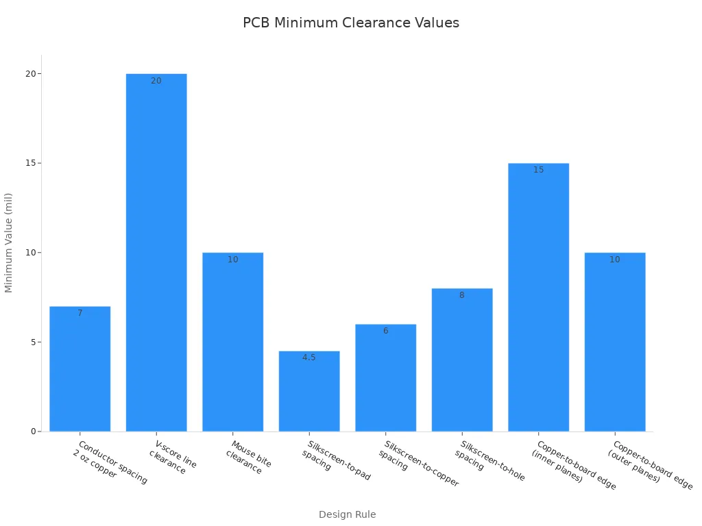
Supporting Memory and Storage
Memory Integration
Your circuit boards host several memory types. Flash stores firmware and configuration data. RAM provides temporary workspace for active processing. EEPROM retains small amounts of data through power cycles. Place decoupling capacitors on top or bottom layers as close to IC power pins as possible. These capacitors drop immediately to internal power and ground planes. This placement ensures stable power delivery to memory chips.
Data Bus Design
Data buses move information between the processor and memory. Route high-speed differential pairs parallel, length-matched, and symmetrical. This ensures common-mode noise rejection. Minimize unnecessary vias because each one introduces an impedance discontinuity. Remove stubbed or unconnected traces on chip nets, especially differential pairs, to prevent signal reflections.
Enabling Edge and Cloud Communication
Gateways and Protocol Translation
An IoT gateway sits at the edge and cloud boundary. It translates southbound field protocols such as Modbus, CAN, Zigbee, and LoRaWAN into cloud-friendly protocols like MQTT, AMQP, and HTTPS. This translation reduces the number of cloud connections and provides a single management point. Your PCBs support both edge processing and cloud connectivity through these gateway functions. Edge computing hosts containerized applications and continues local control during cloud connectivity loss.
Security and Encryption Modules
Security modules on your PCB provide a hardware root of trust. TPM 2.0 and secure elements handle key storage, secure boot, and cryptographic operations. Combine these with TLS mutual authentication, firewalls, and signed OTA updates. This layered approach creates a security perimeter for edge-cloud communication. Your IoT circuit boards gather data from sensors, process it, and send it to other devices or the internet. Power management circuits and supporting components complete the system.
Key Design Considerations for IoT PCBs
Miniaturization and Multilayer Design
High-Density Interconnect Boards
IoT devices demand extremely small footprints. You need fine-pitch components, BGA packages, and high-density interconnect techniques to meet these size constraints. HDI boards use microvias and fine traces to pack more connections into less area. This approach raises connection density without enlarging the board. For compact IoT modules, HDI is often the only way to keep board size under control while meeting functionality goals. A well-planned layer arrangement prevents signal interference and ensures manufacturability. You should start with simpler HDI designs before moving to complex multi-layer boards.
Layer Stackup for Space Savings
Multilayer PCBs help you segregate power and signal traces to address space constraints. A thoughtful stackup increases layer interconnect density without increasing board size. Via-in-pad and fine traces allow more components under fine-pitch ICs. Shorter electrical paths reduce via length and improve return paths. This matters for wireless and high-speed IoT modules. Better impedance control from closely routed traces also supports wireless stability. You should partner with a manufacturer experienced in HDI stackup design and material selection.
Surface Mount Technology
Smaller Components and Denser Layouts
Surface mount technology removes the need for component leads to pass through the board. Components solder directly onto the PCB surface. This shift enables extremely small parts and much closer placement than traditional leaded parts. SMT supports ultra-small packages such as 0201 and 01005. Double-sided population lets you mount components on both sides, doubling usable space without increasing board size. Shorter trace lengths improve signal integrity and reduce EMI, which is critical for high-frequency circuits.
Automated Assembly Benefits
Automated pick-and-place machines achieve micron-level placement accuracy. High-speed machines install thousands of parts per hour with micron-level accuracy. This precision supports consistent production quality for your IoT PCBA. Advanced inspection methods like AOI and X-ray remain important for catching defects such as tombstoning, solder bridging, and BGA voiding. These factors increase manufacturing complexity, so you must plan for inspection blind spots during IoT PCB assembly.
Reliability and Environmental Resilience
Resistance to Environmental Stressors
IoT circuit boards face moisture, vibration, and temperature extremes. In humid conditions above 80% relative humidity, uncoated boards may develop tin whiskers or copper trace corrosion. In high-temperature environments such as automotive compartments exceeding 125°C, thermally resistant coatings prevent degradation. Vibration damping reduces fatigue in leads and traces, which is crucial for automated machinery. Dust and salt ingress are blocked from sensitive areas under intact coatings.
Conformal Coating and Rugged Materials
Conformal coating is a dielectric material applied to assembled PCBs. It shields components and traces from environmental stressors while adding minimal thickness, typically 25 to 250 microns. The coating acts as a barrier that reduces water vapor transmission and prevents ionic contamination. It maintains insulation resistance above 100 megaohms even after humidity exposure. Coatings can extend PCBA operational life by 50% or more in harsh conditions. For your IoT PCB design, these protective measures determine long-term field reliability.
IoT PCB Applications in the Real World
Smart Home Devices
Thermostats and Security Cameras
Your smart thermostat relies on a printed circuit board to gather data from temperature and humidity sensors, run control algorithms, and adjust your HVAC system. The same board hosts the wireless module that lets you change settings from your phone. Security cameras and doorbells use a PCB to power high-resolution image processing and send real-time alerts the moment motion appears. A printed circuit board in IoT devices coordinates microcontrollers, sensors, wireless links, and power supplies inside one compact space.
Voice Assistants and Lighting
Voice assistants need microphone arrays, audio processing chips, and wireless modules working together. The PCB layout determines how cleanly those signals travel. Smart lighting depends on a PCB to regulate LED efficiency and enable dimming or color schedules. Flexible PCBs bend into curved enclosures, which lets these devices shrink without losing circuitry.
Wearable Technology
Fitness Trackers and Smartwatches
Wearables push miniaturization to its limit. An HDI design connects a processor, memory, and Bluetooth module within a compact area. Fine trace widths and microvias pack a 32-bit processor, a 3-axis accelerometer, and an optical heart rate sensor onto a small board. Polyimide-based flexible materials let the board bend with your wrist. Low-resistance copper traces minimize power loss for small batteries, and the total thickness stays minimal.
Health Monitoring Patches
Health patches collect vital signs and transmit them over Bluetooth or Wi-Fi. The PCB must survive constant flexing, so manufacturers test flexible boards through repeated flex cycles. Automated pick-and-place machines calibrated for minimal force handle tiny 0201 resistors. Low-temperature soldering and conductive adhesives prevent thermal stress and delamination.
Industrial IoT
Predictive Maintenance Sensors
Factories use vibration, pressure, and temperature sensors to catch mechanical faults before equipment fails. An IoT PCB supports high-speed digital design, controlled impedance, and RF/wireless routing for these sensor nodes. Eaton worked with Digi to build a predictive monitoring system that predicted hydraulic hose failure before it happened. These systems reduce unplanned downtime and lower maintenance costs.
Asset Tracking and Automation
Asset trackers use RFID, GPS, Bluetooth Low Energy, and NFC to monitor high-value equipment and inventory. Your PCBA enables real-time visibility into production quality, material flow, safety conditions, and energy use. Modern manufacturing runs on unseen PCBs inside smart robotics and factory automation. Wireless modules and gateways feed data to edge processors, and AI-assisted monitoring alerts operators at the first sign of a hazard.
You have seen how a printed circuit board acts as the central hardware platform inside every connected product. The PCB enables connectivity, sensor integration, power management, and data processing. Exploring the role of printed circuit boards in IoT devices shows one clear truth. Thoughtful IoT PCB design determines real-world performance. Miniaturization, multilayer layouts, surface mount technology, and reliability measures all shape the final result. Your PCB choices decide whether a device performs or fails. As IoT grows, PCB innovation will remain essential. Smaller, smarter, and more efficient IoT devices depend on continued PCB advances. Every reliable PCBA starts with a well-planned PCB.
FAQ
What makes an IoT PCB different from a standard circuit board?
An IoT PCB packs sensors, processors, power management, and wireless radios into a severely constrained footprint. Every microamp of leakage current matters. RF integration becomes essential. Standard boards tolerate forgiving spatial margins and accept higher power waste. IoT boards demand careful component selection and disciplined layout to meet size, power, and connectivity goals.
How do PCBs support wireless protocols like Wi-Fi and Bluetooth?
The PCB routes signals between the antenna and radio module. Impedance-controlled traces hold signals on a stable path. A ground plane underneath the antenna trace blocks unwanted noise. Designers place antennas near the board edge, away from metal. These steps reduce degradation for Wi-Fi, Bluetooth, Zigbee, and LoRa links.
Why does sensor placement matter on an IoT circuit board?
Sensor placement determines measurement accuracy. You keep temperature sensors away from power regulators and processors that generate heat. You place motion sensors at the board edge so enclosure walls do not block their field of view. You route analog traces away from high-speed digital lines to prevent noise from corrupting readings.
What role do PCBs play in power management for IoT devices?
The PCB distributes stable voltage to every component. Power and ground planes provide low-impedance paths for return currents. Voltage regulators maintain stable output despite battery changes. Battery management systems monitor voltage, current, and temperature to prevent over-discharge. Decoupling capacitors near power pins stabilize voltage during switching events.
How do PCBs enable edge and cloud communication?
An IoT gateway on the PCB translates field protocols such as Modbus and Zigbee into cloud-friendly protocols like MQTT and HTTPS. Security modules provide a hardware root of trust. TPM 2.0 and secure elements handle key storage, secure boot, and cryptographic operations. This layered approach creates a security perimeter for edge-cloud communication.
What design techniques help PCBs survive harsh environments?
Conformal coating shields components and traces from moisture, vibration, and temperature extremes. The coating adds minimal thickness and maintains insulation resistance above 100 megaohms after humidity exposure. Thermal vias under heat-generating components create low-impedance heat paths. Rugged materials and vibration damping reduce fatigue in leads and traces.
How does surface mount technology benefit IoT PCB assembly?
Surface mount technology removes the need for component leads to pass through the board. Components solder directly onto the PCB surface. This shift enables ultra-small packages such as 0201 and 01005. Double-sided population doubles usable space without increasing board size. Shorter trace lengths improve signal integrity and reduce EMI for high-frequency circuits.
What memory types do PCBs host in IoT devices?
Your circuit boards host several memory types. Flash stores firmware and configuration data. RAM provides temporary workspace for active processing. EEPROM retains small amounts of data through power cycles. You place decoupling capacitors close to IC power pins to ensure stable power delivery to memory chips.
