How to Choose the Right Multilayer PCB for Your Application
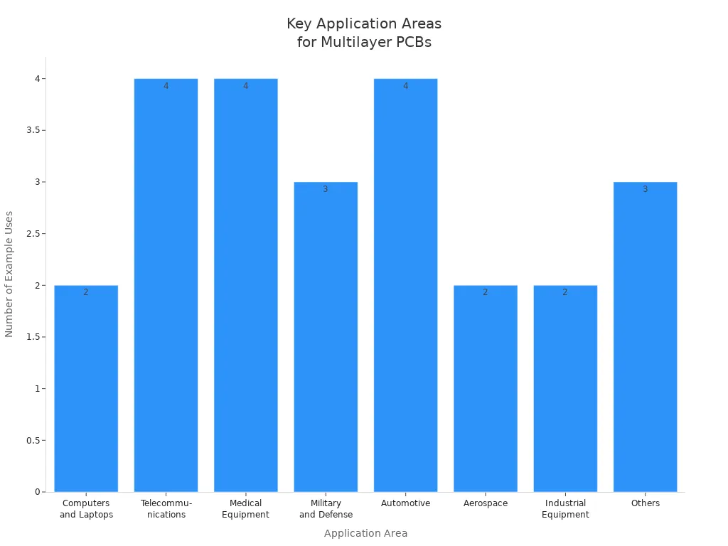
Selecting the right multilayer PCB ensures it aligns perfectly with your project requirements. Multilayer PCB application is essential when dealing with complex circuits, limited space, or when high performance and reliability are critical. These applications play a vital role in advanced electronics across medical, industrial, and telecommunications sectors.
Key Takeaways
Make sure your multilayer PCB’s layers and materials fit your project’s needs. Think about how complex, big, or powerful your project is. This helps your signals stay strong and your device work well.
Use design tools to plan your stackup, vias, and materials. Plan carefully to lower noise and control heat. Careful planning also helps you avoid expensive mistakes before making your PCB.
Pick a trusted supplier like LT CIRCUIT for your PCBs. They check quality, make fast prototypes, and give expert help. This helps you get strong and high-performing multilayer PCBs.
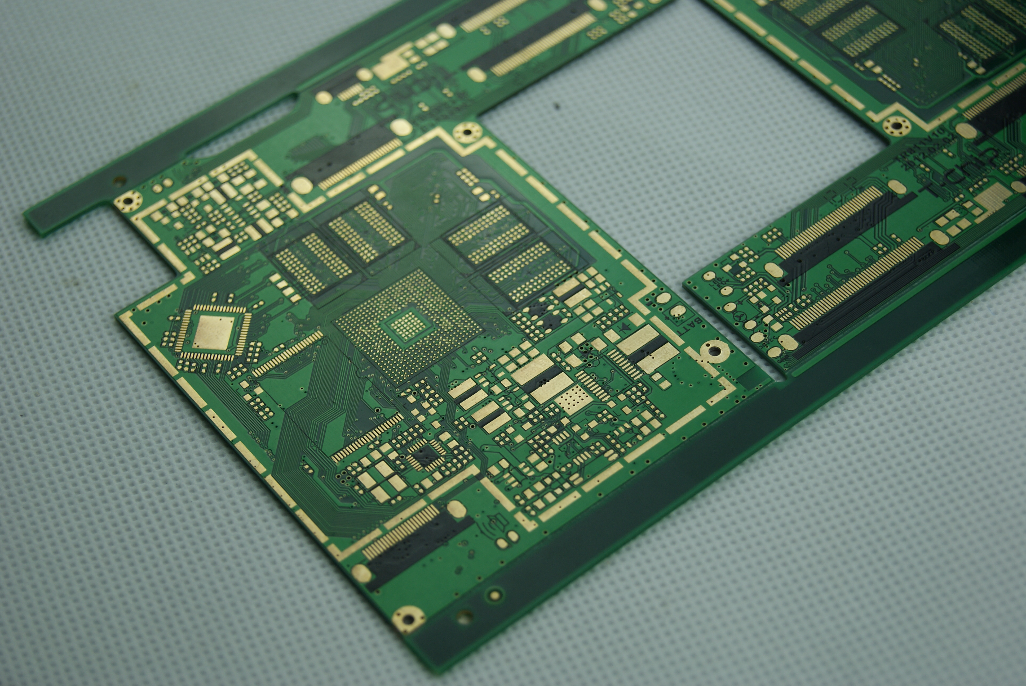
Multilayer PCB Application

Assessing Requirements
Start by thinking about what your project needs. Look at how hard your circuit is. If you have many parts, fast data, or sensitive signals, you need a multilayer pcb application. These boards help you connect tricky circuits. They also cut down on interference and keep signals strong.
Check how much space you have for your pcb. Multilayer pcb application lets you fit more parts in small spaces. This is important for things like smartphones and medical devices. Think about how well your circuit must work. Circuits that use high speeds or are sensitive to noise do better with more layers. Extra layers help block noise and control signals.
You should also think about your budget and how many boards you need. Multilayer pcb application works better but costs more to make. If you make a lot of boards, the cost is worth it because they last longer and break less.
Tip: Always check rules like IPC-2221 and IPC-6012B. These help your multilayer pcb application meet the right standards for your industry.
Here’s a quick look at where multilayer pcb application matters most:
Industry | Applications / Examples | Reasons for Multilayer PCB Use |
|---|---|---|
Consumer Electronics | Smartphones, tablets, laptops, gaming consoles | Compact design, high performance |
Automotive | ADAS, engine control units, infotainment systems | Enhanced functionality, durability |
Medical Devices | MRI machines, pacemakers, diagnostic equipment | High precision, reliability |
Aerospace and Defense | Radar systems, avionics, satellite communications | High reliability, performance |
Telecommunications | High-speed networking equipment, 5G infrastructure, fiber-optic communication systems | Efficient signal transmission, durability |
Layer Count & Complexity
The number of layers in your pcb changes how well your multilayer pcb application works. More layers help you connect hard circuits, give better power, and keep signals clear. Fast or high-frequency circuits need more layers to keep signals apart and stop interference.
Most consumer electronics use 4 to 6 layers to save money and keep things simple. But aerospace, military, and tough jobs may need 8, 10, or even more layers. For example, satellites might use 16-layer boards to stop signal loss and handle heat. Medical machines can need up to 24 layers for accuracy and safety.
Typical Military Application Complexity | Description | |
|---|---|---|
1-2 Layers | Low complexity | Simple control systems and sensors; cost-effective and basic functionality |
3-4 Layers | Moderate complexity | Increased routing flexibility; balance of cost and functionality; space-limited applications |
5-8 Layers | High complexity | High-speed, high-density applications like radar and communication devices; critical performance and reliability |
9-12 Layers | Very high complexity | Complex designs with multiple components; used in avionics and missile guidance systems |
13+ Layers | Ultra high complexity | Specialized, cutting-edge systems such as stealth aircraft and satellite communications |
Pick the right number of layers for your circuit. Too few layers make it hard to connect everything and can hurt signals. Too many layers cost more and are harder to make. Use special design tools to test and plan your multilayer stackup before you finish your pcb.
Note: More layers make signals better by giving more ways to block noise and control signals, but they also need more vias, which must be planned well.
Here are some real-life examples where multilayer pcb application is needed:
Satellite projects use 16-layer boards with Rogers material to keep signals strong.
Medical imaging uses 24-layer boards for safety.
Smartphones and laptops use rigid multilayer boards for small, strong designs.
Cars use multilayer boards for smart circuits.
Wearables and foldable phones use flexible multilayer boards for small size and bending.
Drones and car systems use rigid-flex boards for both strength and bending.
IoT devices use multilayer boards to keep everything lined up and working right.
Size & Form Factor
The size and shape of your pcb matter a lot in multilayer pcb application. Small devices like phones, wearables, and medical implants need tiny, packed boards. These often use HDI, flexible or rigid-flex multilayer boards, and microvias to fit lots of parts in small places. Traces can be as thin as 50 microns, and boards may need to bend without breaking.
Big devices, like desktop computers and machines, use bigger, stiff multilayer boards. These focus on being strong, handling heat, and lasting long instead of being small. You can make these boards bigger, but you still need to think about heat and how hard they are to put together.
Device Type | PCB Form Factor & Size Constraints | Typical PCB Types Used | Key Features & Applications |
|---|---|---|---|
Portable Devices | Compact, high-density, often flexible to fit small enclosures | Thin traces, microvias, flexible boards for wearables, foldables, smartphones. Enables high integration density and compactness. | |
Stationary Devices | Less stringent size constraints, focus on durability and thermal management | Rigid multilayer PCBs | Robust, solid boards for desktops, appliances. Focus on heat dissipation, mechanical strength, and reliability. |
Tip: Odd shapes and very big or tiny boards cost more to make. Standard sizes are easier and cheaper to build.
When you plan your multilayer pcb application, always balance small size with how easy and cheap it is to make. Flexible and rigid-flex boards help in tight spaces, but need special ways to make them.
Multilayer PCB Design Essentials
Material Selection
When you design a multilayer pcb, you pick materials first. FR-4 is used a lot because it is strong and cheap. It also keeps electricity from leaking. If your board needs to work fast, you might use Rogers or PTFE. These help signals stay clear and not get lost. Copper foil makes the paths for electricity. Prepreg layers hold the board together and stop electricity from jumping. If your board gets hot, you can use ceramic or aluminum. These help move heat away and keep the board safe. The table below shows how each material helps with heat and how long the board lasts:
Material Type | Thermal Management | Reliability Impact | Typical Use |
|---|---|---|---|
FR-4 | Limited | Good for most uses | Consumer, automotive |
Rogers/PTFE | Excellent at high speeds | High for advanced applications | Telecom, aerospace |
Ceramic | Excellent | Very high in harsh conditions | Power, sensors |
Aluminum | Excellent | Stable, lightweight | LEDs, power electronics |
Tip: Always choose materials that match your board’s needs. This helps your multilayer pcb design work well and last longer.
Stackup & Signal Integrity
The stackup is how you put the layers together in your board. You place copper and other layers in a special order. This helps control how signals move and stops noise. Putting ground layers next to signal layers keeps signals safe. It gives signals a good path to return and stops interference. Try to keep the stackup the same on both sides. This stops the board from bending. Use computer tools to check your stackup before you build it. For fast boards, follow rules for trace width, space, and layer order. This stops signals from mixing and getting weak. The right stackup also helps power move and keeps your board strong.

Via Types & Routing
Vias are holes that link layers in your board. Through-hole vias are easy and cheap but take up more room. Blind and buried vias let you connect only some layers. This makes your board smaller. Microvias are used in HDI boards for very tight spaces. They cost more but save space. Where you put vias can change how signals move. Too many vias or bad spots can make signals bounce or get lost. Use design software to plan where vias go and how big they are. This keeps signals strong and your board easy to build.
Note: To save money and get good results, pick the best materials, stackup, and vias for your board. Use computer tools to check your design and stop mistakes.
Choosing the Right Supplier: LT CIRCUIT
Quality & Technology
Picking a supplier for your multilayer PCB is important. You want good quality and the best technology. LT CIRCUIT is special because it follows strict rules. The company has certificates that prove it is safe and reliable.
Certification/Standard | Purpose/Role | Relevance to Multilayer PCB Reliability |
|---|---|---|
ISO 9001 | Quality management | Consistent quality control |
IATF 16949 | Automotive quality | Meets automotive-grade requirements |
ISO 13485 | Medical device quality | Ensures safety for medical PCBs |
AS9100D | Aerospace quality | High reliability for aerospace |
IPC-6012 (Class 3) | PCB acceptance | High standards for defense and aerospace |
MIL-STD-202/883 | Military testing | Proves durability in harsh conditions |
JEDEC | Reliability testing | Long-term performance |
RoHS & REACH | Environmental safety | Free from hazardous substances |
LT CIRCUIT uses new ways to make boards. You get high-density interconnect PCBs and laser boring. Microvias help make the boards smaller and better. They use machines to check boards and special soldering. These tools help you get strong and fast boards for any job.
Customization & Support
Sometimes your project needs a special design. LT CIRCUIT lets you pick many options. You can ask for custom multilayer or HDI PCB designs. You can choose different solder mask colors or finishes. The team helps you change designs to control heat and signals. They help with BOM and Gerber files, so making your board is easy.
LT CIRCUIT works with you from the start. You get to see visual prototypes and test your ideas. Early tests find problems before you make many boards. This help saves you time and money. You can fix your design before making the final board.
Tip: Fast prototypes and expert help from LT CIRCUIT stop big mistakes. You can get your product ready faster.
Manufacturer Reputation
You want a supplier with a good history. LT CIRCUIT uses Six Sigma to lower mistakes and make boards better. Machines test the boards to find problems early. The teams have top certificates and use the best tools. You get your boards fast and know they are checked well.
Factor | LT CIRCUIT (Local) | Overseas Manufacturers |
|---|---|---|
Delivery Time | 3–6 weeks plus shipping | |
Quality Control | Strong, easy audits | Harder to audit |
Best For | Prototypes, urgent, high-reliability | High-volume, cost-sensitive |
If you pick LT CIRCUIT, you get a partner who cares about quality. They use new ideas and help customers. You can trust them with your next multilayer PCB design.
To pick the best multilayer PCB, you need to do a few things. First, make sure your stack-up and materials fit your project and budget. Next, use computer tools and ask the maker to check your design. Always choose strong materials and trusted suppliers like LT CIRCUIT for better results.
Check what your project needs often so it works well for a long time.
FAQ

What is the main advantage of using a multilayer PCB?
You get better performance, less noise, and more compact designs. Multilayer PCBs help you fit complex circuits into smaller spaces.
How do you choose the right material for your multilayer PCB?
You should match your material to your speed, heat, and reliability needs. FR-4 works for most uses. Rogers or ceramic suits high-speed or high-heat jobs.
Can LT CIRCUIT help with custom multilayer PCB designs?
Yes! You can work with LT CIRCUIT’s engineers to create custom stackups, finishes, and layouts. They support you from design to final production.
See Also
Exploring Various Industry Uses For Multilayer PCBs
Step-By-Step Guide To Manufacturing Multilayer PCBs
Essential Skills Needed For Designing Multilayer PCB Layouts