The essential steps to produce a multilayer PCB
Learning how to make a multilayer PCB involves following a series of precise steps. First, you need to design the board, select the right materials, and process the inner layers. Next, you move on to lamination, drilling, plating, and outer layer processing. After that, you apply the solder mask, perform surface finishing, inspect the board, and complete the final profiling. If you skip or rush any of these steps while learning how to make a multilayer PCB, you may encounter issues like layer misalignment, drilling burrs, or resin-plugged via defects. These common problems can negatively impact your board’s performance. Understanding how to make a multilayer PCB helps you avoid these mistakes and ensures that every board meets high quality standards.
Key Takeaways
Carefully do each step from design to packaging to make a strong and dependable multilayer PCB.
Pick the best materials and watch over steps like lamination and drilling to stop mistakes.
Check and test your board well to find problems early and make sure it is high quality.
Step by Step Guide to Multilayer PCB Fabrication
When you make a multilayer PCB, you follow steps in order. These steps help you build circuit boards that work well. Every part of making multilayer PCBs is important. If you skip a step or mess up, your board might not work right. You should know the whole pcb fabrication process before you start.
Design and Data Preparation
You start making a multilayer pcb by getting your design files ready. Most companies use Gerber or IPC-2581 formats. You need to check your files for mistakes. Make sure they fit what your fabrication shop needs. Good design helps you avoid problems later.
Set up negative plane layers with the right space.
Change pad shapes for both inner and outer layers.
Update drawings for multilayer printed circuit boards.
Talk to your manufacturer early about things like layer count and via types.
Tip: If you talk to your fabrication shop early, you can save time and money when making multilayer pcbs.
Material Selection
Picking the right materials is very important in making multilayer pcbs. Epoxy resin is used a lot because it sticks well and handles heat. Polyimide is good for boards that need to bend or handle high heat. CFR-epoxy is best for aerospace circuit board fabrication. PTFE is used for boards that need to work with high frequencies. Thermoplastic materials are becoming more popular because they can bend. The material you pick changes how strong and reliable your multilayer circuit board is.
You have to pick materials that match your design and the needs of your pcb manufacturing process. This step makes sure your multilayer pcb fabrication meets industry rules and gives you good results.
Inner Layer Processing
Core Material Selection
You begin by picking the right core materials. The core is the base of your circuit board. You must check different properties before you choose. These properties change how your multilayer pcb works.
Electrical Properties: You want a steady dielectric constant (Dk). This keeps signals strong, even when they move fast. High resistivity stops signals from leaking out.
Thermal Properties: Pick a core with a high glass transition temperature (Tg). Good thermal conductivity helps the board handle heat. These things stop the board from bending or warping.
Mechanical Properties: The core should be tough and not break or bend. Strong cores keep your multilayer circuit board safe from harm.
Environmental and Chemical Resistance: Choose a core that does not soak up water or get hurt by chemicals. This helps your board last longer in hard places.
Note: For high-speed or RF circuit boards, you need a core with a tight Dk and low water absorption. For power boards, focus on thermal conductivity and insulation.
You also need to follow environmental rules. Many companies use RoHS-compliant and halogen-free materials. This makes pcb manufacturing safer and better for the earth.
Cleaning and Preparation
Before you image the inner layers, you must clean the core. Dust, oil, or dirt can cause problems in multilayer pcb manufacturing. Use isopropyl alcohol to clean off oils. Use demineralized water for light dirt. For tough dirt, use special pcb cleaners.
Use soft brushes or air to blow away dust.
Wear gloves so you do not touch the board with oily hands.
Keep cleaned cores in containers with no dust.
These steps stop rust and water problems. Clean rooms are best for this job. If you skip cleaning, you might get defects that ruin your board.
Imaging and Etching
Now you put your circuit pattern on the inner layers. Cover the core with a dry film that reacts to light. Use UV light or a laser to show the pattern. After this, you develop the film. The parts not shown to light wash away. The copper traces stay safe under the film.
Next, you remove the extra copper by etching. Chemicals like ferric chloride, ammonium persulfate, and cupric chloride are used. Each chemical has its own safety and earth rules. For example, cupric chloride can be used again, which cuts down on waste.
Here is a table with common imaging and etching facts:
Aspect | Details |
|---|---|
Photoresists, UV exposure, laser direct imaging | |
Etching Chemicals | |
Quality Control Methods | Automated Optical Inspection (AOI), manual inspection |
Defects Detected by AOI | Shorts, opens, spacing errors, pattern distortions |
Registration Accuracy | Maintained within < 5 mil tolerance |
Tip: Keeping the right temperature and moving the chemicals helps you get even etching and fewer mistakes.
Etch Stripping
After etching, you must take off the leftover photoresist. This is called etch stripping. Use chemicals like sodium hydroxide to do this. Always wear gloves and goggles to stay safe. Good airflow is needed because some chemicals make fumes.
Ferric chloride works well but is hard to throw away safely.
Cupric chloride is better for the earth and can be used again.
Hydrogen peroxide and hydrochloric acid are safer for the planet.
Many factories now use closed systems to recycle chemicals and cut down on waste. This makes multilayer pcb manufacturing safer for people and the earth.
Inner Layer AOI
When you finish etching and stripping, you must check for mistakes. Automated Optical Inspection (AOI) scans the board and checks it against your design. AOI finds problems like shorts, opens, and pattern mistakes. This step is very important because you cannot fix inner layer mistakes after lamination.
AOI can find up to 90% more mistakes than people can. But AOI cannot see inside the layers. Some companies use X-ray checks for hidden problems. If AOI finds a mistake, you must decide if you can fix the board or throw it away.
Remember: Careful checking now helps you avoid big mistakes later in pcb manufacture.
Oxide Treatment and Layup
Oxide Treatment
You must treat the copper on the inner layers first. This step is called oxide treatment. Chemicals like brown or black oxide are used. These chemicals make the copper surface rough. The rough surface helps the prepreg resin stick better during lamination.
Oxide treatment is needed for a strong multilayer circuit board. If you skip this, the layers may not stick well. Bad bonding can make the layers come apart. This can cause the circuit board to fail. Oxide treatment helps copper and resin bond tightly. This makes the peel strength higher. Experts say it should be over 5 pounds per inch for 1oz copper foil. You also control how much oxide is on the copper and how long the crystals are. These things stop delamination and make your multilayer pcb more reliable.
Factor | Effect on Adhesion |
|---|---|
Peel Strength | Stronger bonding |
Oxide Weight | Better layer adhesion |
Crystal Length | Improved resin bonding |
Tip: Always check the chemical strength and timing. This helps you get the best results for your circuit board.
Layer Stackup
After oxide treatment, you do the layer stackup step. You put the treated inner layers, prepreg sheets, and outer copper foils in order. How you stack these layers changes how your multilayer circuit board works.
A normal stackup for a 6-layer pcb is:
Top Signal Layer
Ground Plane
Internal Signal Layer
Power Plane
Ground Plane
Bottom Signal Layer
This setup keeps signals and power balanced. Ground planes next to signal layers help signals return easily. This lowers noise and stops electromagnetic interference. If you have more layers, you add more signal and plane layers. You keep the stackup even on both sides. This stops the board from warping and keeps it flat.
You also set the space between layers with core and prepreg materials. The space is important for impedance control and making boards smaller. A good stackup design helps your board work at high speeds. It also lowers crosstalk and keeps electrical performance steady.
Lamination
Heat and Pressure Bonding
Lamination is a key step in making a multilayer circuit board. You put all the layers together in a stack. Then you use heat and pressure to join them into one board. The stack goes inside a vacuum press. This machine takes out air and stops bubbles from forming.
You set the temperature between 180°C and 200°C. The pressure should be between 300 and 500 psi. These settings help the resin move and fill every space. The right heat and pressure make the resin harden well. This keeps the board strong and stops it from bending or coming apart. The stack stays in the press for 60 to 120 minutes. The time depends on how many layers your board has.
Parameter | Standard Range | Why It Matters |
|---|---|---|
Temperature | 180-200°C | Cures resin, prevents warping and delamination |
Pressure | 300-500 psi | Bonds layers, removes voids |
Time | 60-120 minutes | Ensures full curing for all layers |
Tip: Always watch the lamination process closely. If you use the wrong settings, you can get problems. These include layers coming apart, small white spots, or bubbles. These issues can happen if the resin is not even, the materials are bad, or there is too much water.
After lamination, check the board to see if it is bonded well. You should not see any gaps or bubbles. Good lamination makes your multilayer pcb strong and ready to use.
Drilling
Via and Hole Creation
You must make holes and vias to link the layers. This step uses special drilling machines. There are two main ways to drill. One is mechanical drilling. The other is laser drilling. Each way has good and bad points.
Description | Typical Hole Diameter | Tolerance (Diameter) | Depth Control Tolerance | Advantages | Disadvantages | |
|---|---|---|---|---|---|---|
Mechanical Drilling | Uses rotating carbide steel drill bits to create holes through PCB layers. | ~0.010 inch | ±0.003 inch | Older machines: ±0.002 inch | High quality, consistent holes; sharp edges; suitable for larger vias and through-holes. | Drill bits can break for very small holes (<0.008 inch); requires deburring; slower for many holes. |
Modern machines: ±0.0005 inch | Controlled depth drilling enables precise blind vias. | Manual setup on older machines is time-consuming; tool changes needed for multiple sizes. | ||||
Laser Drilling | Uses high-intensity laser beams (UV or CO2) to ablate holes, especially for small blind/buried vias. | Smaller than mechanical | Not explicitly quantified | Depth control less accurate | Can create smaller holes; faster processing; non-contact; automated; good for blind/buried vias. | Depth accuracy challenges; tapering of holes; carbonization of edges; less suitable for large holes. |
Mechanical drilling is best for big holes and most through-holes. It makes sharp and neat holes. New machines use cameras and sensors to guide the drill. This helps keep the holes the right size and depth. The depth can be controlled very well, even better than ±0.0005 inches. Laser drilling is used for tiny blind or buried vias. It is fast and can make lots of holes at once. But it is harder to control how deep the holes go.
Mechanical drilling with depth control is used for blind vias.
Special drill bits help make the right hole shape and size.
Newer machines make drilling more accurate and faster.
Not every factory has these machines, but they help a lot.
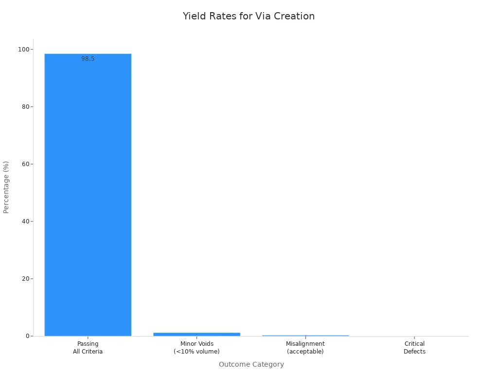
Most vias and holes should meet the quality rules. In a group of 1,000 vias, about 98.5% pass all checks. Only a few have small voids or are a little off-center. Big problems almost never happen.
Metric | Value |
|---|---|
Sample Size | 1000 vias |
Vias Passing All Criteria | 98.5% |
Minor Voids (<10% volume) | 1.2% |
Misalignment (acceptable) | 0.3% |
Critical Defects | 0% |
Tip: Always check your drilling machines and drill bits before you start. Clean tools and a good setup help you get the best results for your multilayer PCB.
Plating and Via Formation
Copper Plating
Copper plating joins all the layers in your multilayer PCB. You must do a few steps to cover every hole and surface with copper. Here is what you do:
Pretreatment: First, clean the copper foil and holes. This takes away oil, dirt, and resin from drilling. Clean copper helps new copper stick well.
Plasma Etching: Next, use plasma to clean and smooth the holes. This also removes tiny burrs that could cause trouble later.
Charge Adjustment: Then, change the charge on the resin surface. This helps the activator stick to the board for the next step.
Electroless Copper Plating: Now, put a thin copper layer on the hole walls and surfaces. This layer is thin and easy to break, but it makes the holes able to carry electricity.
Electrolytic Copper Plating: After that, use electricity to add more copper. This makes a strong copper layer on the holes and both sides of the board.
Pattern Plating: Last, cover places you do not want to plate with a special resist. Then, plate copper only where your circuit needs it.
Tip: Add dummy pads, called thieving, in empty spots. These pads help keep the plating current even. Even current gives the board the same copper thickness everywhere.
Critical Control | Why It Matters |
|---|---|
Oil Removal | Stops dirt and helps copper stick |
Charge Adjustment | Makes copper layer even and connects well |
Thieving (Dummy Pads) | Keeps copper thickness the same |
Plating Current Monitoring | Stops copper from being too thick or too thin |
You need to watch every step carefully. If you skip or rush a step, copper may be uneven or weak. Careful copper plating keeps your multilayer PCB strong and working well.
Outer Layer Processing
Outer Layer Imaging
You begin by putting your circuit pattern on the top and bottom of the board. First, you spread a photoresist layer over the outer copper. Then, you shine UV light through a mask that shows your circuit design. The parts hit by the light get hard. The parts not hit by light stay soft.
Here are the main steps for outer layer imaging:
Photoresist Application: Cover the board with a thin photoresist layer.
UV Exposure: Shine UV light through a patterned film to show your circuit.
Developing: Wash away the soft photoresist, leaving your pattern.
This process makes very thin lines and spaces. Good imaging is needed for your circuit to work right. If you mess up, you could get shorts or open spots.
Tip: Always check your imaging tools and films before you start. Clean tools help stop dust and mistakes.
Outer Layer Etching
After imaging, you start etching. You use chemicals to take away copper not covered by the hard photoresist. This step shows the final traces and pads on your board.
Put the board in an etching machine.
The chemicals remove the extra copper.
Only copper under the photoresist stays.
Careful etching keeps your traces the right size and space. If you do this step well, your board will match the design and work right.
Step | Purpose |
|---|---|
Imaging | Puts circuit pattern on outer layer |
Etching | Takes away extra copper |
Note: Automated Optical Inspection (AOI) usually comes after etching. AOI finds problems like misaligned parts or shorts early, so you can fix them before moving on.