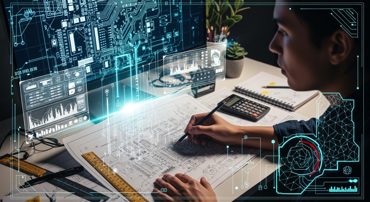
Understanding PCB Engineering Drawings Made Simple
You can learn to read PCB Engineering Drawings by using easy steps. When you know these drawings, you help stop mistakes and slowdowns in your electronics projects. Good paperwork makes your work easier and helps you do better. Many new designs have trouble because drawings are not clear, like charts that do not match or missing information. By learning this skill, you make your projects quicker and more correct.
Key Takeaways
Knowing PCB engineering drawings stops mistakes and makes projects faster.
Learn about different PCB drawings, like assembly drawings and schematic diagrams, to work better.
Always look at the title block in a PCB drawing for important details like part numbers and sizes before you begin.
Use clear steps with assembly drawings to put parts in the right place and not make mistakes.
Practice reading and making schematics to get better at fixing problems and designing good circuits.
What Are PCB Engineering Drawings?
Purpose and Importance
PCB engineering drawings help you build electronic boards. These drawings show where each part goes and how to connect them. They help you not make mistakes. They also help you work faster and get things right. When you use these drawings, you can check your work. You can make sure everything matches the plan.
PCB engineering drawings do many important things in electronics:
They tell you how to put parts on the board.
They give rules so you do not make mistakes.
They help you check if parts are in the right spot.
They help you work with other people, like designers and builders.
These drawings are like a bridge from design to making the board. They have all the details you need to build something real. When you use them, your whole team knows what to do. This helps stop mistakes and keeps your project on track.
Tip: Always look at the drawings before you start building. This helps you find problems early.
Types of PCB Drawings
You will find different PCB drawings in your work. Each one has its own job. Some show where parts go. Others show how to connect wires or check the board.
Here are some common types:
Assembly Drawings: Show where each part goes on the board.
Schematic Diagrams: Show how parts connect to each other.
Fabrication Drawings: Give details for making the board itself.
You should know about the rules for these drawings. These rules help everyone use the same way to draw. Here is a table with two important rules:
Standard | Description |
|---|---|
ASME Standards | Tell how to design mechanical things, like PCB size and shape. |
IPC Standards | Use ASME rules to help make and check electronic products. |
When you learn about these types and rules, you can read any PCB drawing easily.
PCB Assembly Drawings Explained
Key Information in Assembly Drawings
You use pcb assembly drawings to help put parts on a circuit board. These drawings have clear pictures and notes. They show where each part goes and how to place it. You find important details in these drawings, like:
Assembly needs, such as which solder paste to use or special tests
Handling and packaging steps, including moisture and ESD safety
Pictures, like 3D views of the board
Notes about solder paste, handling, and packaging
Assembly views that help you see mistakes in part placement or direction
Steps for adding wires, cables, or enclosures
Pcb assembly drawings focus on the physical part of building a board. They do not show how parts connect in a circuit. Schematic diagrams do that job. Schematic diagrams show how electricity moves, but assembly drawings show where to put each part.
Here is a table that shows how pcb assembly drawings are different from other drawings:
Type of Drawing | Content Description | Purpose |
|---|---|---|
PCB Assembly Drawing | Focuses on component placement, orientation, and assembly process requirements. | Guides actual PCB assembly and production. |
PCB Design Files (Gerber) | Contains layer data for copper traces, pads, and silkscreen. | Used by manufacturers to fabricate the bare board without components. |
Schematic Diagram | Illustrates electrical connections between components, representing circuit logic. | Does not show physical placement, focusing instead on the electrical design. |
BOM (Bill of Materials) | Lists component models, quantities, and suppliers. | Used for procurement and part verification, lacking spatial information. |
Tip: Always check the assembly drawing before you start. This helps you avoid mistakes with part direction or placement.
How to Use Assembly Drawings
You follow easy steps to use pcb assembly drawings at work:
Keep the drawing neat and simple to read. Do not let lines or notes cross.
Check if the drawing shows part polarities, like which way diodes or chips face.
Look for board size and hole sizes.
Read any special assembly instructions.
Make sure you use the newest drawing version.
Read all notes for extra tips or warnings.
Talk with your manufacturer early if you have questions.
These steps help you build the board the right way. Good drawings help you work faster and make fewer mistakes.
How to Read and Create PCB Schematics
When you learn to read and make pcb schematics, you see how circuits work. You start by looking at the symbols in the diagrams. Each symbol stands for a part, like a resistor or battery. You use these symbols to build or fix circuits.
Schematic Symbols and Standards
You will see many symbols in a schematic. Each symbol means something special. The table below shows some common symbols you might see:
Component Type | Symbol Description |
|---|---|
Resistor | Shown as a zig-zag line. |
Capacitor | Drawn as two lines, one may be shorter for polarity. |
Inductor | Looks like curved bumps or a spring. |
Transistor | Drawn as a three-legged part with arrows. |
Diode | Looks like a triangle pointing to a line. |
Integrated Circuit | Shown as a rectangle with many leads. |
Battery | Drawn as long and short lines for positive and negative. |
Ground | Looks like lines that get shorter, showing ground. |
Most schematics use the IEEE Std 315 standard. This standard tells you how to draw the symbols. You can trust these symbols to mean the same thing in most drawings.
Reference Designators
You will see small codes next to each part in a schematic. These codes help you match the drawing to real parts on the board. Here is how they work:
Each part gets a label called a reference designator.
A resistor uses 'R', a capacitor uses 'C', a diode uses 'D', a transistor uses 'Q', and a connector uses 'J' or 'P'.
These labels help you find parts in other documents, like the bill of materials.
You use these codes to check your work and avoid mistakes.
Power and Ground Connections
You should always look for power and ground symbols in a schematic. These connections are very important. They keep your circuit safe and working well.
Good power and ground connections stop ground loops, which can cause noise.
Good grounding helps your circuit avoid signal problems.
Shared ground points keep high-frequency noise away from sensitive parts.
Tip: Always check power and ground first when you read a schematic. This step helps you find problems early.
How to Read and Interpret a Schematic Diagram
Following Signal Paths
First, you trace the signal paths in a schematic. This helps you see how electricity moves between parts. You look for where signals come in and go out. You follow the lines that join the symbols. You check how current moves through each part. You can use a multimeter to check voltage at different spots. This tool helps you find problems in the circuit.
Using datasheets for parts and tools like multimeters is important. These help you design and fix circuits.
Here is a simple guide to help you follow signal paths:
Find where signals enter and leave the circuit.
See how current moves through the circuit.
Figure out how the circuit works by following the flow.
You can use a table to see why following signal paths helps:
Benefit of Following Signal Paths | Description |
|---|---|
Quick Identification of Issues | Schematics give a big picture view. This helps you find problems fast. You can spot power or signal paths quickly when something breaks. |
Systematic Reading | Big projects have many pages of schematics. Reading them in order helps you avoid guessing and saves time. |
Voltage Measurement Insights | Knowing where voltage should change helps you find broken parts fast. |
You also check for polarity in the circuit. Some circuits have both positive and negative charges. You remember that same charges push away and different charges pull together. This idea helps you know how the circuit works.
Cross-Referencing Components
You need to match each symbol in the schematic to the real part on the PCB. You use codes like R1 for resistors or C2 for capacitors. You set up the schematic from left to right or top to bottom. You put related parts close together. You line up parts on a grid to keep things neat.
Label each part with its code and value.
Set up the schematic in a way that makes sense.
Line up parts on a grid to keep it clear.
Put related parts together.
Try not to cross wires and use dots for junctions.
Use standard symbols so everyone understands.
You can check rules that help you match parts:
Standard | Description |
|---|---|
IPC-2221 | General rules for PCB design, layout, and materials. |
IPC-2612/2612A | Rules for making PCB drawings clear and easy to read. |
IEC 60617 | Shows symbols for diagrams so everyone knows what they mean. |
IEEE 315 | Gives lots of symbols for electrical diagrams to keep things clear. |
ISO 128-20 | Gives rules for technical drawings, including schematics. |
When you learn to read and understand a schematic, you can follow signal paths and match parts easily. You get better at solving circuit problems.
Read PCB Engineering Drawings: Step-by-Step
You can learn to read pcb engineering drawings if you use simple steps. This section gives you easy tips to help you not make mistakes. You will see how to start with the title block, find parts and connections, and read notes. These steps help you build good pcb projects and make your job easier.
Start with the Title Block
The title block is at the bottom or corner of each pcb drawing. You should always look here first. The title block gives you important facts about the pcb and the drawing. When you read pcb engineering drawings, check these things first:
Part Title: Tells you the name of the pcb or assembly.
Company Information: Shows which company made the drawing.
Size: Tells you how big the pcb is.
Drawing Number: Helps you find and track the drawing.
Part Number: Shows the special number for the pcb part.
Scale: Tells you how the drawing size matches the real pcb.
Drawn: Names the person who made the drawing.
Projection: Tells you the drawing method used.
Weight: Shows how heavy the pcb is.
Sheet: Tells you which page you are looking at.
Material: Lists what the pcb is made from.
Finish: Tells you about the surface finish on the pcb.
Application: Explains where the pcb will be used.
Tolerance: Shows how much the size can change.
Tip: Always check the revision and scale in the title block. This helps you not use old drawings and makes sure you have the right size.
Identify Components and Connections
You need to find and understand every part and connection on the pcb drawing. This step helps you build the pcb right and not make mistakes. When you read pcb engineering drawings, do these things:
Mark Top and Bottom Sides: Find out which parts go on the top and which go on the bottom. This stops mix-ups when you build the board.
Check Polarity: Look for parts like diodes, LEDs, and electrolytic capacitors. Use the + and - signs to put them in the right way.
Indicate Rotation: Make sure you see the right direction for parts like ICs, connectors, and polarized capacitors. Pin 1 marks for ICs help you place them right.
You should also use a checklist to check each part of the pcb design and making. This checklist helps you find mistakes early and keeps things correct:
Check raw materials before you start.
Watch the making steps during production.
Check where parts go during assembly.
Test the board to make sure it works right.
Note: Checking at different steps helps you find mistakes before they get worse. Always double-check where parts go and which way they face.
Interpret Notes and Callouts
Notes and callouts give you extra rules and warnings. You must read these carefully so you do not make mistakes. Here is how you read them:
Make sure the title block has key facts like part name, revision, scale, drawing number, material, tolerance, and finish.
Use the same drawing symbols and follow rules like ASME Y14.5 to keep things clear.
Read notes that tell you how to read sizes and tolerances. Look for units and tolerance rules.
Use the right IPC standard for your pcb, like IPC-6012 for rigid boards.
Make sure notes do not go against the IPC standard. If they do, the drawing is more important.
Keep notes simple and only write what you need. This keeps the drawing easy to read and up-to-date.
You can stop common mistakes by doing these things:
Follow DFM Guidelines: Use your manufacturer's DFM checklist early to keep clearances right.
Perform DFM Checks: Use CAD software with DFM tools to find problems before making the board.
Collaborate with Manufacturers: Talk to your pcb maker early to make sure your design fits their tools.
Conduct Peer Reviews: Ask other engineers to check your work. They might find mistakes you missed.
Test Prototypes Thoroughly: Use test tools to check if the board works and if fast signals work right.
Simulate Environmental Conditions: Test boards in different conditions to make sure they last.
Tip: A good checklist from start to finish helps you avoid mistakes. Add checks to your work steps to make things faster and help you trust your pcb designs.
You can read pcb engineering drawings better when you use these steps. This guide helps you build better pcb projects and not make expensive mistakes.
Troubleshooting and Common Mistakes
Typical Errors in PCB Drawings
You can stop many problems if you know common mistakes. Most errors happen when people design or check PCB drawings. Here is a table that shows some usual errors you might see:
Error Type | Description |
|---|---|
Unconnected nets | Wires do not join pins. This makes signals or power incomplete. |
Pin assignments mismatch | Schematic symbols do not match datasheets. This causes parts to not work right. |
Inadequate power decoupling | Missing capacitors or placing them far from ICs makes voltage drop. |
Duplicate part designations | This confuses assembly and slows down getting parts. |
Wrong resistor or capacitor values | This changes how the circuit works and affects testing. |
Improper component placement | This can cause signal problems and make parts get too hot. |
Poorly designed power distribution | This makes voltage drop and the board work badly. |
You might see these mistakes in assembly drawings too. Unconnected nets can make circuits act weird. Pin mismatches can make boards not work. Bad power decoupling can cause noise in digital lines. Duplicate part names confuse people building the board. Wrong values change how your circuit works. Assembly drawings help you find these mistakes before you build.
Tips for Accurate Interpretation
You can use smart steps to read assembly drawings the right way. Follow this checklist to avoid mistakes:
Keep mechanical and assembly layers apart. This makes drawings easier to read.
Show polarities clearly. Mark cathodes, anodes, and pin 1.
Add board outline and sizes. Give all measurements in your drawings.
Label special needs. Write notes for things like coating.
Track changes. Mark versions in your drawings.
Add helpful notes. Give clear instructions, not just short hints.
Talk to your manufacturer early. Share drawings before you finish your design.
Always check your assembly drawings twice. This helps you find mistakes before you build. Design rule checks look for problems like trace width, spacing, and pad size. These checks make sure your drawings follow all rules.
You can use a table to help you fix problems:
Step | Verification Method | Pass Criteria |
|---|---|---|
Net Connectivity | Run ERC for opens/shorts | No big violations |
Pin Assignments | Check datasheets | All pins match the part |
Power Decoupling | Count caps per IC | At least 0.1uF per power pin |
Reference Designators | Unique across sheets | No repeats and in order |
BOM Export | Make and check | Values and tolerances listed |
Annotation Completeness | Full sheet coverage | No nets without labels |
If you see noise or signal problems, check for missing grounds or connections. Fixing these early saves time and money. Good drawings help you build strong PCBs every time.
You can get good at PCB engineering drawings by using easy steps. Learn how to spot parts, read schematic symbols, and follow circuits. Practice with real PCB drawings to help you see where things go. This makes your technical skills, problem-solving, and focus better. Use the right tools and label each part so you do not make mistakes. If you want to learn more, check out these resources:
If you practice a lot, you will understand and fix PCBs more easily.
FAQ
What is the difference between an assembly drawing and pcb schematics?
You use an assembly drawing to see where each part goes on the board. You use pcb schematics to understand how parts connect. Assembly drawings help you build the board. Pcb schematics help you follow the flow of electricity.
How do I start reading circuit board schematics?
You start by learning the symbols in the schematic. You look for power and ground first. You follow the lines to see how signals move. You use these steps to create a pcb schematic and understand circuit board schematics.
What are the main steps to create a pcb schematic?
You gather all parts for your circuit design. You draw each symbol in the schematic. You connect the symbols with lines. You label each part. You check your work. These steps to create a pcb schematic help you avoid mistakes.
Why is an assembly drawing important for assembly?
An assembly drawing shows you where to place each part. You see the correct direction for parts. You use the drawing to check your work during assembly. This drawing helps you avoid errors and makes assembly faster.
What are some tips for efficient schematic design and troubleshooting with schematics?
You keep your schematic neat and simple. You use clear labels. You follow tips for efficient schematic design like grouping related parts. You use troubleshooting with schematics by checking connections and looking for missing parts. You practice creating schematics to get better.
See Also
Key Skills Required for Mastering Multi-Layer PCB Layouts
Comprehensive Overview of Flexible PCB Production Techniques
Exploring LT CIRCUIT's Capabilities in Complex PCB Fabrication
Understanding PCB Printed Circuit Boards and Their Fundamental Principles