What is an IC Package Substrate and Why It Matters in Chip Packaging
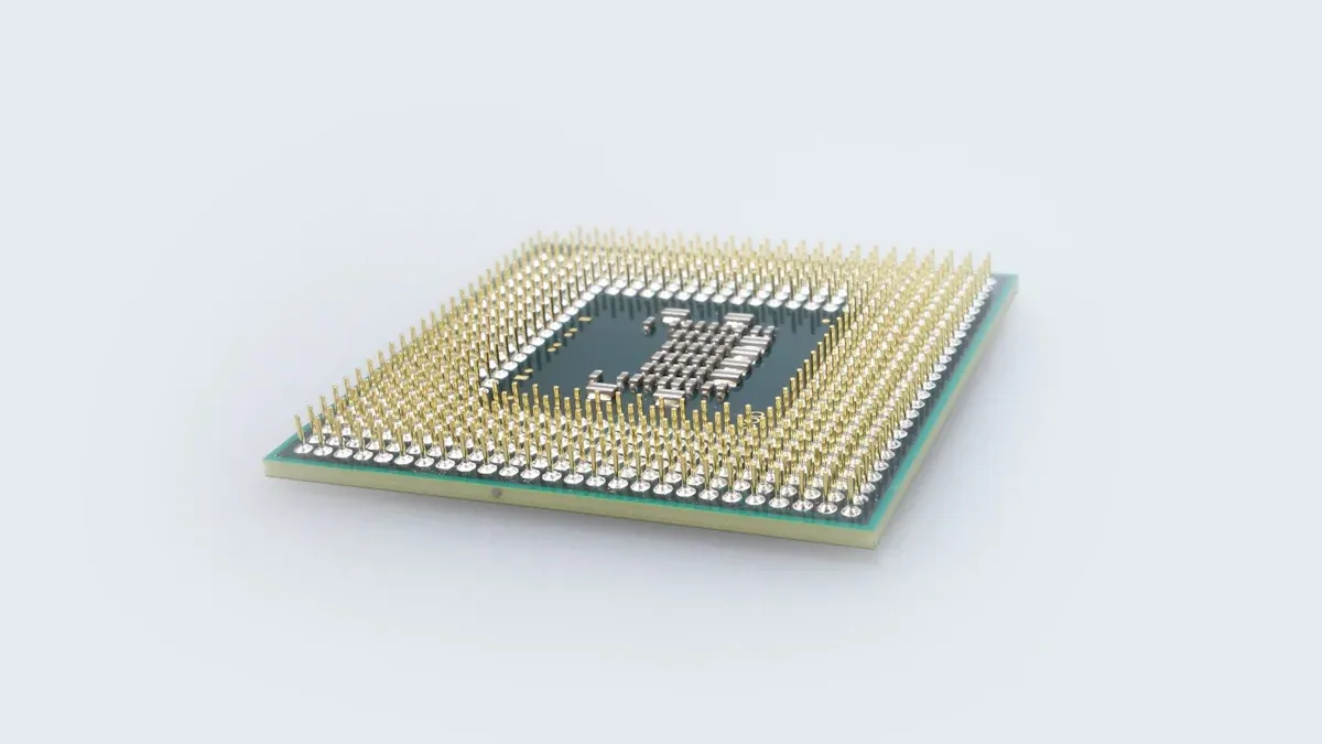
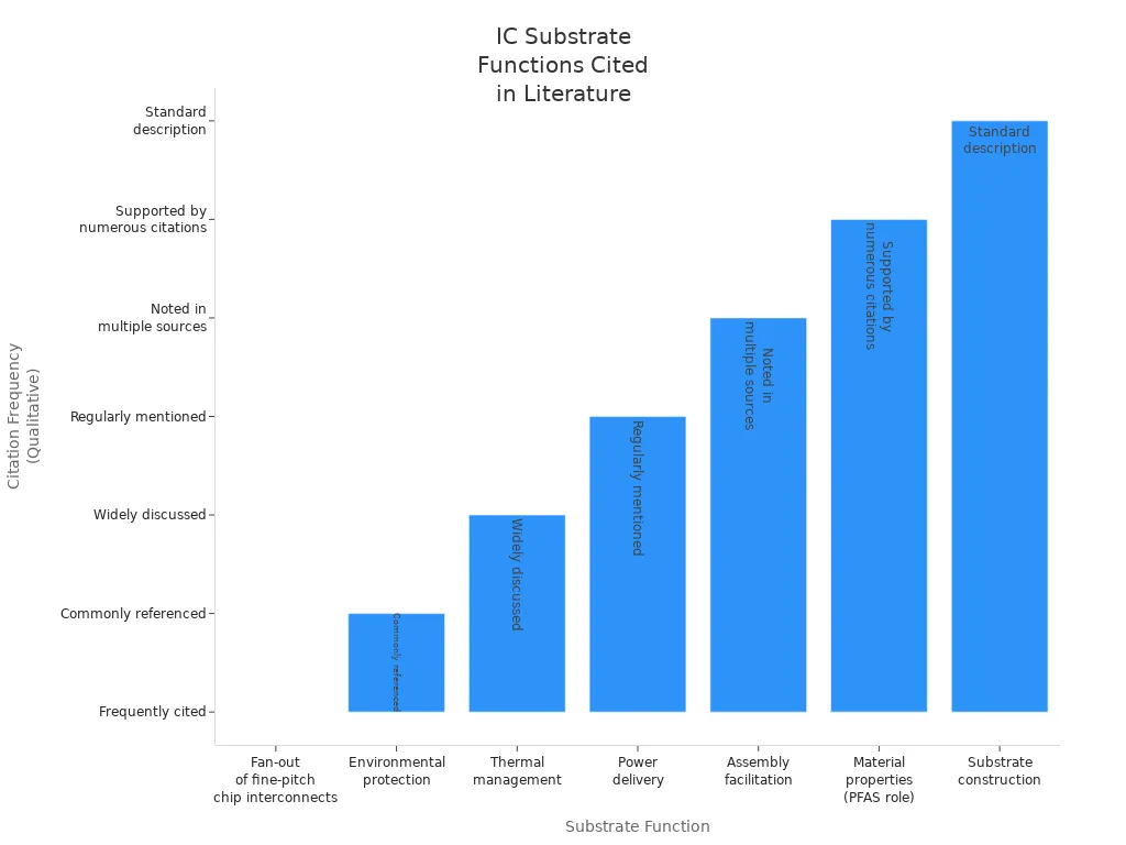
An ic package substrate is a key link between the ic chip and the printed circuit board. It gives electrical connections and holds the chip in place. It also spreads signals the right way. The substrate helps send power to the chip and cools it down. This makes it very important for chip packaging. The table below lists the main jobs of an ic package substrate in packaging:
Function / Role | Description / Details |
|---|---|
Fan-out of fine-pitch chip interconnects | Changes small chip connections to bigger ones for the printed circuit board. This lets the chip work with the board. |
Environmental protection | Keeps the chip and its connections safe from things like water and dirt. |
Thermal management | Moves heat away from the chip to keep it working well. |
Power delivery | Gives steady and good power to the chip through the substrate. |
Assembly facilitation | Makes it easier to put together without needing super clean rooms. This helps make chips faster. |
Material properties (PFAS role) | PFAS materials help by not letting much water in. They also have low permittivity and low dielectric loss. They are strong, stick well, resist chemicals, and move heat well. |
Substrate construction | Uses many layers and tight wiring with organic laminates or ceramics. |
Key Takeaways
IC package substrates link the chip to the circuit board. They help signals move fast and clear. They also give steady power. This helps devices work well and last longer.
They keep chips safe from harm and heat. They use strong materials and smart designs. This keeps electronics safe and working, even in hard places.
Picking the right substrate material and design makes devices faster, smaller, and stronger. This is important for gadgets like smartphones, cars, and AI systems.
IC Package Substrate Functions
Electrical and Signal Connections
An ic package substrate is the main path for electrical signals. It connects the ic chip to the printed circuit board. This lets the chip talk to other parts in a device. The substrate has thin copper lines and special paths. These help signals move fast with little loss. Flip chip technology puts the die right on the substrate. It uses copper microbumps for this. This makes the electrical path shorter. Signal delays are much less than with wire bonding. Flip chip can cut delays by up to 75%. It also lets more signals in and out and helps with heat.
The table below shows how different packaging methods compare for signal connections:
Packaging Method | Parasitic Inductance (nH) | Parasitic Capacitance (pF) | Power Density (W/mm²) | Signal Integrity |
|---|---|---|---|---|
Flip Chip | 0.5 | 0.3 | 10 | High |
Wire Bonding | 5.0 | 1.5 | 5 | Medium |
BGAs | 3.0 | 1.0 | 7 | Medium |
CSP | 1.0 | 0.5 | 8 | High |
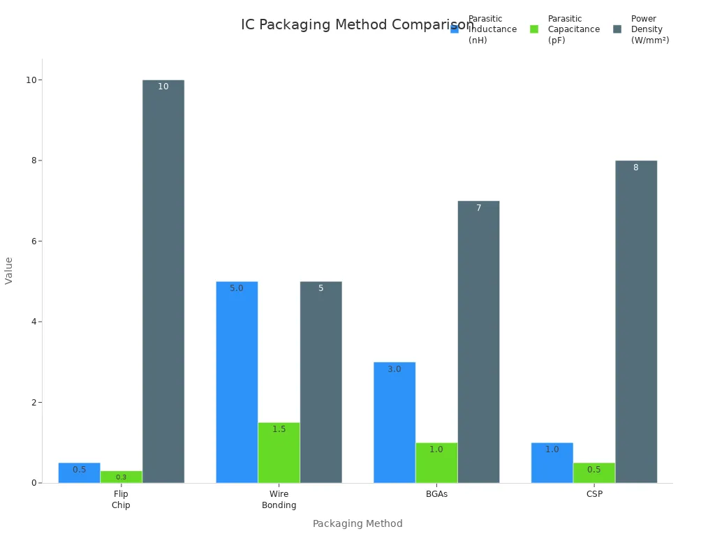
The ic substrate helps keep signals strong and clear. It stops signal loss and blocks interference in fast circuits. Makers use coreless substrates and hidden traces to lower unwanted effects. They pick materials with low dielectric constants. They also use careful copper patterns. These things help keep signals good, even when chips are packed tight.
Coreless substrates lower unwanted effects and make signals better.
Hidden traces stop signal loss and block bad signals.
Many layers in the substrate let signals travel in complex ways.
Low dielectric materials keep signal delays short in fast circuits.
The ic substrate lets the chip send and get signals fast and safely. This is very important for modern chips, especially those that need to work at high speeds.
Mechanical Support and Protection
The package substrate is a strong base for the ic chip. It holds the chip steady and keeps it safe from harm. The substrate must handle stretching, bending, and shaking. It cannot break or lose its grip on the chip.
Parameter/Condition | Value/Description |
|---|---|
Maximum tensile strain with module-specific substrate | Up to 600% strain without delamination or failure |
Tensile strain causing delamination in stretchable module (weak adhesion) | 100% tensile strain |
Tensile strain causing delamination in stiff module (modulus mismatch) | 200% tensile strain |
Maximum Mises stress on conventional homogeneous substrate at 200% strain | 12.46 MPa |
Maximum Mises stress on module-specific substrate at 200% strain | 4.65 MPa |
Cyclic deformation endurance | 15,000 cycles at 70% strain (stable operation) |
Operational strain for LED in integrated circuit | LED remains lit up under 400% stretch; failure beyond due to electrical breakdown of conductors |
The ic substrate uses ceramics and organic laminates to be strong. It works with an encapsulant, usually epoxy resin. This covers the chip and keeps out dust and water. Together, they help the chip stay safe and work well, even in tough places.
Note: The package substrate and encapsulant make a safe space for the ic chip. They guard against bumps, heat changes, and dirt. This helps the chip last longer.
Industry rules, like JEDEC and Mil-STD-883, say substrates must pass hard tests. These tests check for damage from heat, water, and force. Engineers use special tools to find weak spots and make things better. These steps make sure the ic substrate can be used in important devices, like those in planes or hospitals.
Power and Heat Management
The ic package substrate helps give power to the chip and move heat away. It uses special shapes and materials to spread power and cool the chip. Insulated metal substrates (IMS) are good at moving heat away from the chip. This keeps the chip cool and helps it last longer.
Thermal vias let heat move between layers fast.
Heat sinks soak up heat and let it out, working with vias.
Ceramics and special plastics help spread heat well.
EMI shields block bad signals and keep power steady.
Via-in-pad designs let more parts fit and make the substrate stronger.
Materials in ic substrates, like thermal interface materials, have different heat-moving abilities. Most are a few W/(m·K) up to about 6 W/(m·K). Some, like indium, can go much higher. Better heat movement means cooler chips and better work.
The substrate also helps with new ways to give power. Flip-chip and BGA use direct links and solder balls. This makes the path for power and heat shorter and better. Microvias and fine paths let many parts fit close together and still work fast.
The ic substrate makes sure the chip gets steady power and stays cool. This is very important for powerful chips, like CPUs and GPUs, where too much heat can break them.
Types and Structure of IC Substrate
Package Substrate Materials
Organic substrates and ceramic packages are the main types used. Organic substrates are cheaper and easy to make. They are common in things like smartphones and smartwatches. Ceramic packages are stronger and handle heat better. Engineers use them for powerful chips or tough places. Organic substrates are getting better with new technology.
Material | Key Properties | Pros | Cons | Cost and Performance Impact |
|---|---|---|---|---|
Excellent dielectric, low signal loss, good thermal stability | Great for high-speed, high-density circuits | Higher cost, complex processing | High cost, top performance | |
BT Resin (Bismaleimide-Triazine) | Good thermal stability, strong insulation | Balanced cost and performance | Lower heat control than ceramics | Cost-effective, mid-range uses |
Ceramics (Alumina, AlN) | High heat control, strong, good insulation | Best for power and heat | Expensive, brittle | Most costly, best for tough jobs |
The material you pick changes how small and strong chips can be. Ceramics help small chips stay cool and safe. Organic materials let designers make thin and bendy gadgets.
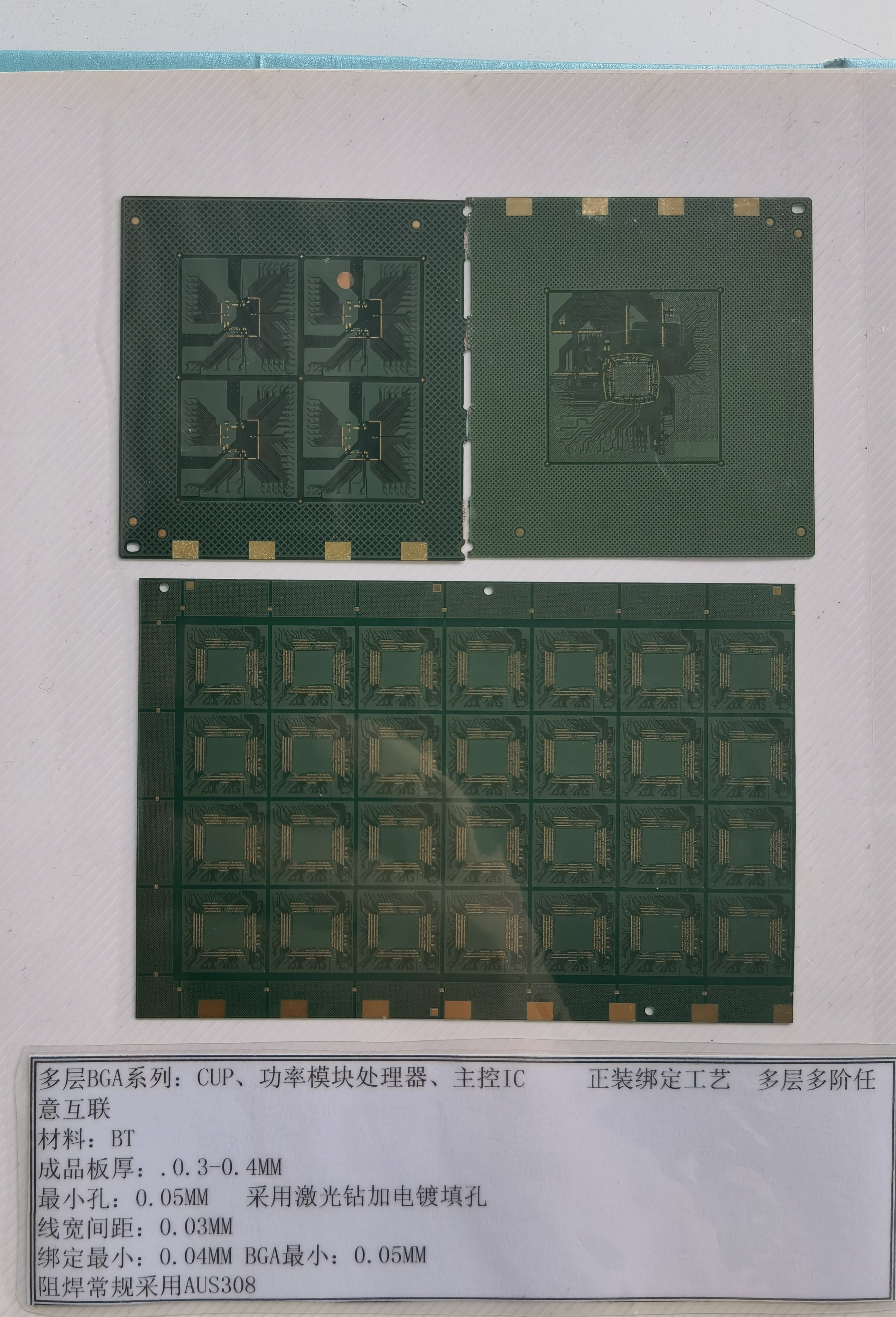
Integrated Circuit Substrate Manufacturing
Making an ic substrate takes many careful steps. First, workers put copper foil and resin films together. They drill tiny holes for connections. Next, they add copper and use light to make patterns. More layers are added with resin and copper. They drill microvias for tight connections. At the end, they coat it, finish the surface, and test everything.
Note: Making ic substrates uses special tools like lasers and UV lights. These tools help make the tiny lines and shapes needed for new chip packaging.
IC Substrate vs PCB
IC substrates and PCBs look alike but are not the same. IC substrates have thinner layers and very tiny lines. They use blind and buried vias. PCBs have thicker layers and bigger lines. IC substrates let chips attach right to them. PCBs hold bigger, ready-made parts.
Feature | IC Substrate | Standard PCB |
|---|---|---|
Layer Thickness | Very thin | Thicker |
Via Types | Blind, buried, microvias | Through-hole |
Line Width/Spacing | <25 microns | >80 microns |
Integration | Direct die, fine pitch | Larger parts, coarse pitch |
Fabrication | Advanced (laser, UV, additive) | Subtractive etching |
IC substrates give better signals and heat control. They also help connect lots of tiny parts. This makes them important for new chip packaging.
Real-World Applications
IC substrates are used in many devices. In phones, they help fit more power in less space. Memory chips use them to keep data fast and safe. Cars and planes use ceramic substrates for strength and heat control. Data centers use them for fast chips with clear signals.
IC substrate helps make devices smaller by fitting more circuits.
Ball grid array and chip-scale package make devices faster and stronger.
The type of substrate affects heat, signals, and how long devices last.
IC substrates are found in gadgets, medical tools, and space tech. They are more important as new things like 5G and AI need better chips.
IC package substrates help make today’s electronics better. They let devices work faster and last longer. They also help make gadgets smaller. Experts say packaging is important for AI, cars, and data centers. New ways to package chips, like chiplets and fan-out panel-level packaging, help control heat. More people now know why packaging matters. This helps engineers, makers, and users.
Packaging technology helps 5G, healthcare, and electric cars grow. Engineers and makers use packaging to build smaller and quicker devices. These devices are also more reliable.
FAQ
What is the main difference between an IC substrate and a PCB?
IC Substrate | PCB |
|---|---|
Finer lines | Thicker lines |
Fewer layers | |
Smaller size | Larger size |
Why do engineers use ceramic substrates?
Ceramic substrates are good at handling heat. They keep chips safe in tough places. Engineers pick them for power devices, cars, and planes.
Can IC package substrates affect device speed?
Yes. Substrates with tiny wires and special materials help chips send signals faster. This makes devices work better and react quickly.
See Also
Exploring IC Substrate PCBs And Their Essential Roles
Comparing Full In-House Versus Partial In-House PCB Production
A Comprehensive Guide To ENEPIG In PCB Fabrication