IC Package Substrate versus PCB: What Sets Them Apart
You must pick between IC Package Substrate and PCB when making electronics. Each one has special strengths for signal quality, heat control, and making things smaller. Engineers use these differences to work better and meet what the market wants, as you can see in the chart below.
Metric/Aspect | Value/Description |
|---|---|
Market Size (2024) | USD 15.1 Billion |
CAGR (2025-2033) | 10.51% |
Key Growth Drivers | AI, 5G, EV platforms, flip-chip adoption |
Key Takeaways
IC package substrates join single chips with small, quick paths for electricity. They also control heat very well. This helps make devices smaller and stronger.
PCBs connect many parts in a device with bigger lines. They use easier materials. This makes building electronics cheaper and dependable.
You pick between an IC package substrate and a PCB based on your design needs. Think about size, speed, heat control, and money to make the best device.
Definitions
IC Package Substrate
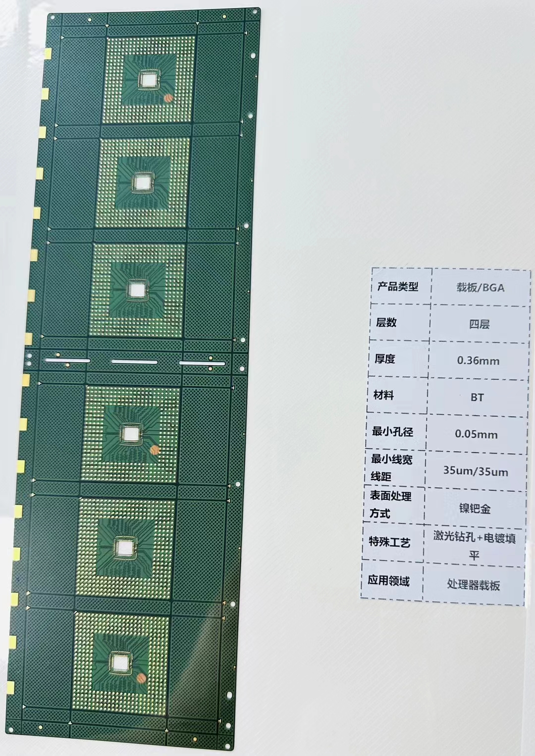
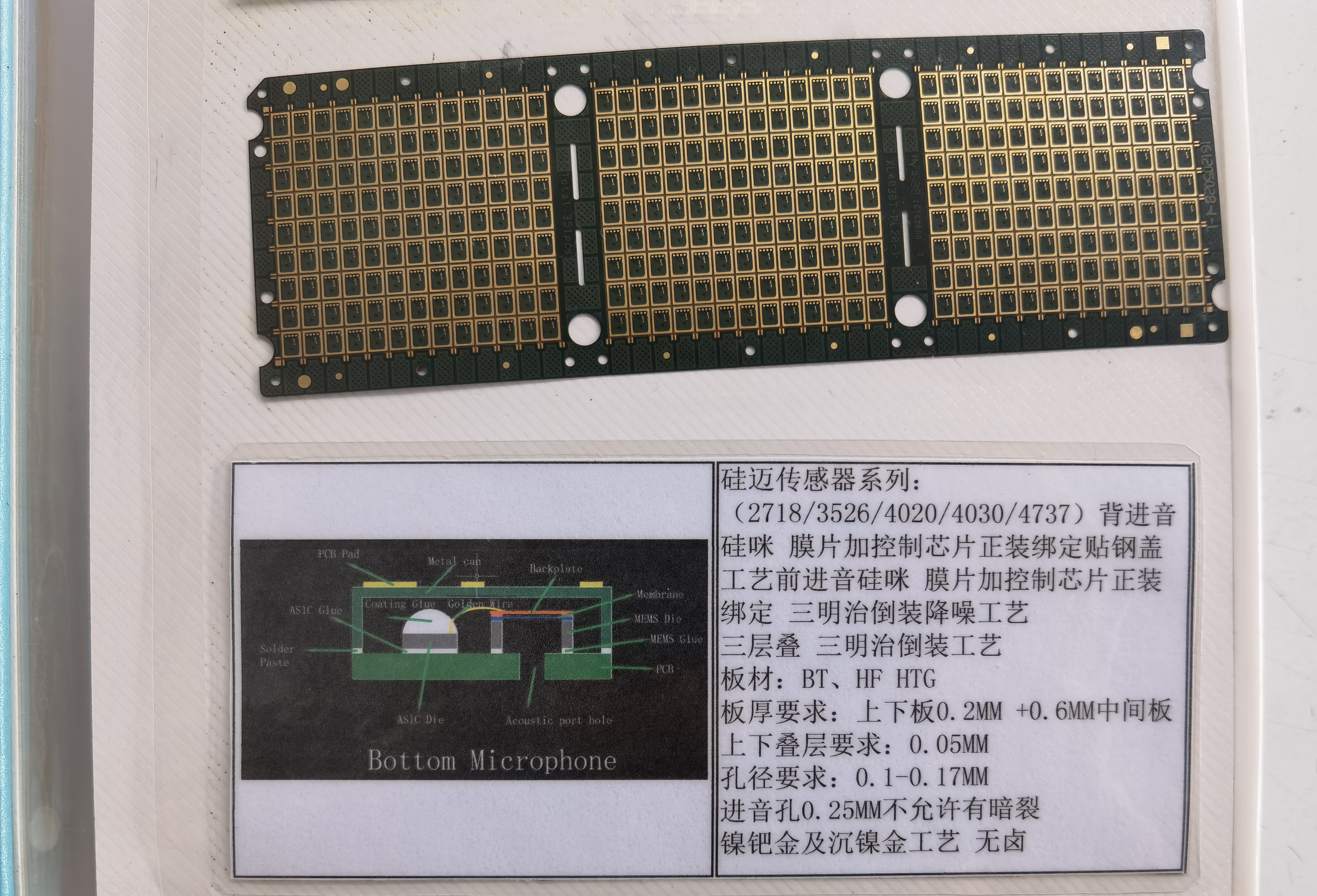
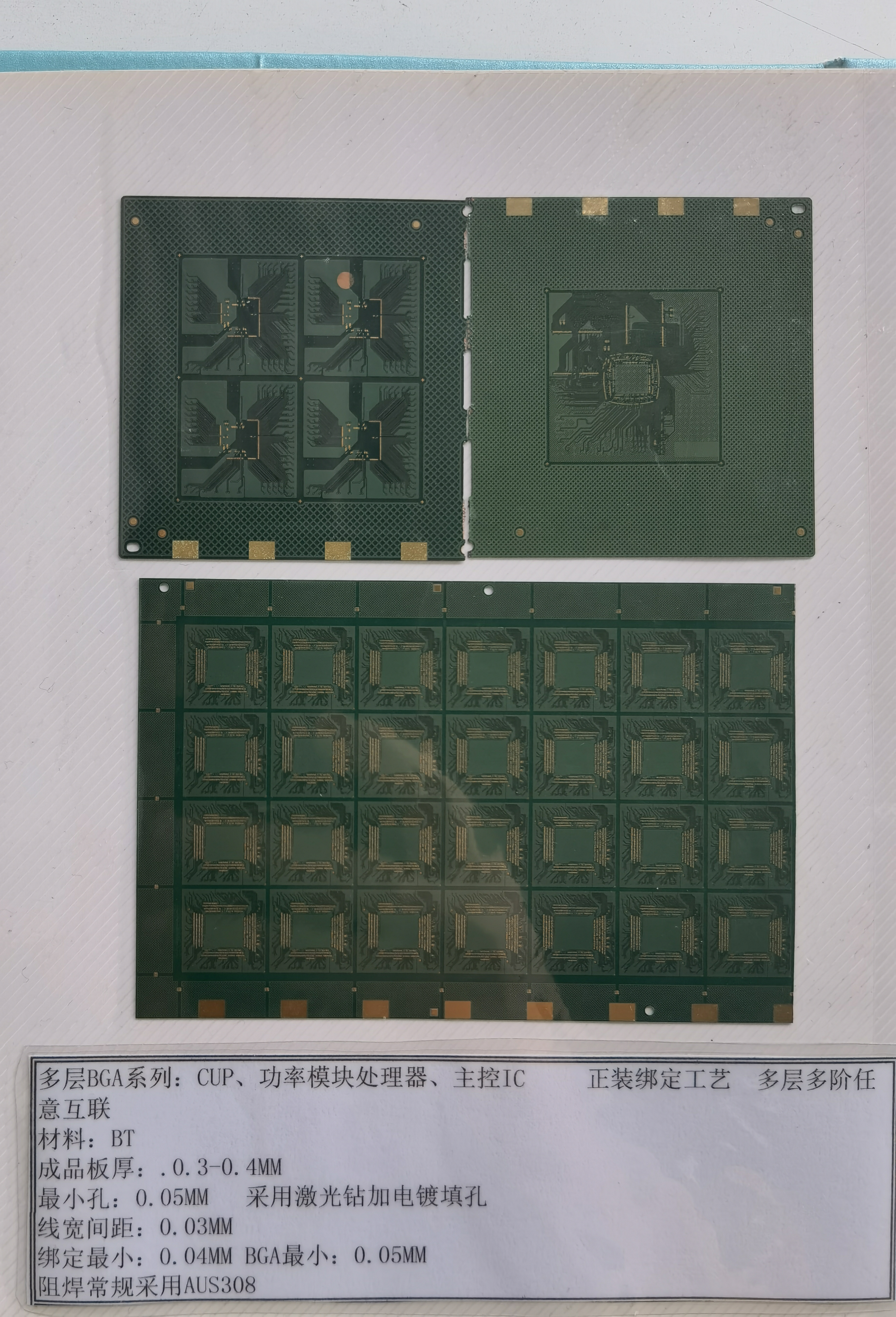
An IC package substrate connects a chip to a printed circuit board. It gives electrical connections and holds the chip in place. Experts say the substrate helps signals move well and keeps the chip steady. These substrates have many layers of special materials. This lets them handle lots of tiny wires and send signals fast. These things are important for new electronics. In flip chip packages, the substrate holds the chip with solder bumps. This setup gives power, heat control, and support. You often see glass, organic laminates, or ceramics used. These help the substrate move heat and electricity better. The IC package substrate also cools the chip, protects it, and helps with new ways to put chips together, like 3D stacking. These features help you make small, powerful designs.
Tip: If you want more power and speed in less space, use an IC package substrate.
PCB
A PCB is the main part of almost every electronic device. It looks like a flat board with copper and other layers. Copper lines connect parts like resistors, capacitors, and chips. You attach these parts to pads on the board. Small holes called vias let signals go between layers. PCBs can have one, two, or many layers. This depends on how hard your circuit is. The board holds the parts and connects them with wires. You find PCBs in phones, computers, cars, and medical tools. They help machines put parts on boards quickly. PCBs help you make strong, small, and cheap electronics.
Industry Sector | Main Functions of PCBs | Application Examples |
|---|---|---|
Help car electronics and safety systems | Navigation, engine control, parking sensors | |
Medical Devices | Give safe electronics for health care | Imaging, monitors, pacemakers |
Consumer Electronics | Make small, strong circuits for daily gadgets | Smartphones, computers, home appliances |
Industrial Equipment | Tough, powerful electronics for factories | Factory machines, power equipment |
Key Differences
There are some big differences between an IC package substrate and a PCB. The substrate uses much smaller lines, sometimes only 12 micrometers wide. PCBs have bigger lines and spaces. The substrate has more layers and uses special materials for better performance. It is usually smaller and made for fast, high-power jobs like flip-chip assemblies. PCBs are bigger and connect many parts in a device.
Aspect | IC Package Substrate | PCB |
|---|---|---|
Feature Size | Very small lines and spaces (down to 12µm) | Bigger, wider lines |
Layer Count | Many layers, special structures | Fewer layers, less packed |
Material Focus | Great at moving electricity and heat | Made to save money and insulate |
Application | Used for small, powerful chip packages | Used to connect many parts |
Size | Smaller (like 15x15mm to 55x55mm) | Larger boards |
Cost | Costs more because of advanced uses | Costs less, made in big amounts |
You use the IC package substrate to connect a chip to other parts with speed and trust. You use a PCB to connect many parts in a bigger system. Your choice depends on what you want your design to do, how well it must work, and how much you can spend.
Structure & Materials
Density & Layering
IC package substrates and PCBs are built in different ways. IC package substrates can have up to 14 layers. Most PCBs only have 2 to 6 layers. More layers mean you can fit more connections in less space. The lines and spaces in IC package substrates are much smaller. Some can have a bump pitch of 150 micrometers or even less. PCBs have wider lines and spaces. This means they cannot fit as many connections in the same area.
Parameter | IC Package Substrates | Substrate-Like PCBs (SLP) / HDI PCBs |
|---|---|---|
Typical Layer Count | 2 to 14 layers (e.g., Intel 65-nm: 12 layers; 45-nm Atom: 6 layers) | 2 to 6 layers, advanced up to 6+ layers |
Line/Space (Interconnect Density) | Bump pitch down to 150 µm or less (flip-chip bump pitch) | Line/space down to 30/30 µm; advanced 20/20 µm; SAP process can reach 15/15 µm |
Via Diameter | Laser-ablated micro-vias, via-in-pad techniques | Laser-defined vias around 50 µm diameter |
Materials | High Tg BT resin, low CTE, build-up processes | BT resin (Bismaleimide Triazine), high Tg (250-300°C), low CTE (2-5 ppm/°C) |
Process Techniques | Build-up substrate fabrication, semi-additive and subtractive patterning | Semi-additive (mSAP, SAP), subtractive, laser via drilling |
IC package substrates use very thin layers and tiny microvias. These help make fine-pitch connections for fast chips. You can use them for advanced packaging. PCBs use thicker layers and bigger vias. This makes them good for regular electronics but not for very dense or fast circuits.
Material Choices
Picking the right materials is important for your design. IC package substrates use special materials like ABF, BT resin, and sometimes ceramics. These materials give better insulation, handle heat well, and are strong. Some substrates use ceramics like LTCC or HTCC for even better heat control. These choices help keep signals clean and manage heat, which is needed for fast chips.
PCBs usually use FR4, which is fiberglass mixed with epoxy resin. FR4 is strong, cheap, and easy to use. It works for most electronics but does not handle heat or fast signals as well as IC package substrate materials.
Material Type | Common Materials in IC Package Substrates | Common Materials in PCBs |
|---|---|---|
Organic Substrates | ABF (polyimide-based), BT resin, high Tg, low CTE | FR4 (fiberglass cloth with epoxy resin) |
Ceramic Substrates | LTCC, HTCC (multi-layer ceramics) | N/A |
Specialized Features | Fine pitch routing, high integration, thermal management | General mounting, cost-effectiveness |
Note: IC package substrates often use copper foil that is only 1.5 to 25 micrometers thick. PCBs use thicker copper, usually 18 to 35 micrometers. Thinner copper lets you make smaller lines and features.
Miniaturization
IC package substrates help you make smaller and stronger devices. They support advanced packaging like 2.5D and 3D stacking. You can stack chips on top of each other to save space and boost performance. Thin lines, thin layers, and tiny vias help fit more into less space. This is important for smartphones, AI chips, and car electronics.
Regular PCBs use a flat, 2D layout. They work well for bigger boards and simple designs. But they cannot be as small or packed as IC package substrates. Miniaturized substrates give better signal paths, faster speeds, and better heat control.
Feature | Advanced Packaging Substrate (APS) | Traditional PCBs |
|---|---|---|
Integration Dimension | Supports 3D stacking, vertical integration | 2D layout, simple placement |
Signal Routing Complexity | Intricate, multi-layered pathways | Straightforward 2D traces |
Materials Used | Specialized (organic, ceramic, glass) | Common (FR-4) |
Size and Miniaturization | Smaller, high-density packages | Larger, less compact |
Thermal Management | Efficient heat dissipation | Less optimized |
Application Focus | High-performance, compact devices | General electronics |
🛠️ Tip: If you want high performance and small size, pick an IC package substrate. It helps you make tiny and advanced designs.
Manufacturing
IC Package Substrate Process
Making an IC Package Substrate takes many careful steps. First, you design the circuit and pick materials like BT resin or ABF film. You use photolithography to print the pattern on the material. Next, you remove extra copper to show the paths. Lasers make tiny holes called microvias. These holes help connect the layers together. Thin copper is added with special plating. Gold plating stops rust and keeps signals strong. You must work in a cleanroom to keep dust away. When finished, you test the substrate with X-rays and microscopes. This process needs skilled workers and careful control.
Specialized Equipment/Technique | Description |
|---|---|
Makes very small holes for fine connections | |
Ultra-thin Copper Foil | Allows tiny circuit lines |
Advanced Inspection | Uses X-ray and SEM for quality checks |
Note: Making an IC Package Substrate uses stricter rules and better tools than making a regular PCB.
PCB Process
To make a PCB, you start with a design and pick FR4 as the main material. You print the pattern with a special film. Chemicals remove extra copper from the board. Drilling machines make holes for parts and vias. You cover these holes with copper to connect the layers. A solder mask is added to protect the board. Labels are printed on the board. Machines put the parts on, and soldering joins them to the board. You check the board with visual and machine tests. PCB making is less strict and uses bigger features than IC Package Substrate making.
Process Stage | Description |
|---|---|
Imaging & Etching | Forms circuit patterns |
Makes and coats holes | |
Solder Mask & Labels | Protects and marks board |
Assembly & Testing | Places parts and checks quality |
Cost & Complexity
IC Package Substrate manufacturing costs more and is harder to scale. The process uses advanced materials and has more steps. You must control every detail to stop mistakes. This makes it slower and more expensive. PCB manufacturing is simpler and faster. It uses cheaper materials and can make many boards at once. If you need high performance and small size, you pay more for the IC Package Substrate. If you want lower cost and easy production, you choose a PCB.
Applications
IC Package Substrate Use
IC package substrates are used in many high-tech things. They connect and hold single chips like memory, processor, MEMS, and RF chips. You can find them inside smartphones, laptops, tablets, and printers. They are also important in telecom gear, factory machines, and car electronics. Medical tools, space systems, and military gear use these substrates for steady work. In fast communication devices, IC package substrates help signals stay quick and clear.
Smartphones, laptops, tablets, printers
Telecom and network equipment
Factory machines and car electronics
Medical, space, and military systems
Advanced packaging, like flip-chip and system-in-package, needs these substrates. They give strong support, quick connections, and good heat control. This helps you make smaller and stronger devices.
PCB Use
PCBs connect many electronic parts in one system. They hold and link chips, resistors, capacitors, and more. You see PCBs in almost every electronic thing you use each day.
Application Category | Common PCB Applications | Description |
|---|---|---|
Smartphones, tablets, TVs, computers, home appliances | PCBs power and control your daily gadgets and appliances. | |
Industrial Electronics | Factory equipment, drills, solar power generators | PCBs do tough jobs in factories and power systems. |
Automotive Electronics | Sensors, control systems, navigation, radios | PCBs help cars work safely and well, even in hard places. |
PCBs let you add lots of parts and layers to a system. They help you make strong, flexible, and steady electronics.
Integration
Sometimes you need to connect new chips to old systems. Substrate-like PCBs help you do this job. These special boards mix features from IC package substrates and regular PCBs. They have layers, small holes, and pads for conductors. You can use them to link new chips with normal PCBs. This bridge lets you make smaller and faster devices. Substrate-like PCBs also work with new packaging, like flip-chip and wire bonding, while still fitting with old parts.
Tip: If you want to mix new and old tech, substrate-like PCBs are a great choice.
Performance
Signal Integrity
Good signal integrity is important for fast electronics. IC package substrates have very thin lines and tiny vias. These help signals stay clear and lower noise. You get fewer mistakes and less signal loss, even at high speeds. PCBs have wider lines and bigger spaces. This works for most devices but not the fastest chips. If you need the best signal quality, use an IC package substrate for important parts.
Thermal Management
You need to control heat to keep electronics safe. IC package substrates like BGA and CSP use special pads and thermal vias. These move heat away from the chip fast. Underfill in flip-chip packages gives more ways for heat to escape. It also helps stop stress. PCBs can handle heat well too, if you use metal-core boards or thick copper. You can add thermal vias and heat sinks to spread heat out. Some advanced PCBs use cooling channels or special materials like graphene to cool even more.
IC package substrates move heat away from the chip fast.
PCBs spread heat over the whole board and use extra cooling.
Both help keep high-power devices cool and safe.
Tip: Use the right substrate and PCB design together for the best heat control.
Reliability
You want your devices to work well for a long time. IC package substrates have some special problems. When things heat up and cool down, materials can grow or shrink at different rates. This can cause stress and make cracks or layers split apart. You can lower these risks by picking the right materials and making good heat paths. PCBs have fewer layers and are simpler, so they have fewer of these problems.
Reliability Challenge | What It Means for You |
|---|---|
Can cause cracks or layers to split in substrates | |
Makes warping and splitting more likely | |
Complex Bonding in 3D Packages | Makes it harder to keep bonds strong over time |
Wafer Thinning | Thin chips can crack or bend more easily |
Remember: Good design and smart material choices help your electronics last longer.
Why It Matters
Technology Trends
Every year, new technology changes how you design electronics. Devices keep getting smaller, so you must fit more parts in less space. Miniaturization and HDI help you put more on each board. Flexible and rigid-flex PCBs let you make foldable phones and wearable gadgets. You can hide parts inside boards to save space and make 5G and IoT devices work better.
New materials like ceramics and Teflon help with heat and fast signals. Many companies now try to make PCBs safer for the planet. They use lead-free solder and recycle old boards. Advanced packaging, like SiP and MCM, lets you put many chips together in one package. This makes your devices faster and smaller. 3D printed electronics let you make new shapes and test ideas quickly.
Miniaturization and HDI help make smaller designs.
Flexible and rigid-flex PCBs let you build new shapes.
Embedded parts make devices work better.
New materials help control heat and signals.
Eco-friendly PCBs help protect the planet.
SiP and MCM let you put more chips together.
3D printing helps you test ideas fast.
System Impact
You need to know the difference between IC package substrates and PCBs. IC package substrates hold and connect single chips. They give strong electrical links and help with heat. PCBs connect many chips and parts. They are the main support for your device.
Using advanced substrates gives you better signals and faster data. Good heat control keeps chips cool and working longer. New types like substrate-like PCBs and HDI boards help you make smaller and stronger products. Knowing these jobs helps you balance size, speed, and reliability.
Tip: If you pick the right substrate and PCB, your electronics will be smaller, faster, and last longer.
You now see how IC package substrates and PCBs serve different needs. PCBs connect many parts in your device. Substrates support single chips and help with speed and heat. Think about your design goals and material needs.
Want to learn more? Explore advanced packaging and PCB technology for your next project.
FAQ
What is the main job of an IC package substrate?
You use an IC package substrate to connect a chip to a board. It helps signals move fast and keeps the chip cool and safe.
Can you use a PCB instead of an IC package substrate?
No, you cannot. A PCB connects many parts in a device. An IC package substrate connects only one chip to the board.
Why do IC package substrates cost more than PCBs?
Reason | IC Package Substrate | PCB |
|---|---|---|
Material Quality | Higher | Standard |
Feature Size | Smaller | Larger |
Manufacturing Steps | More | Fewer |
You pay more for better materials and finer features.
See Also
Understanding IC Substrate PCBs And Their Main Roles
Comparing Full In-House Versus Partial In-House PCB Production
Choosing The Right PCB Materials For Communication Devices
Exploring Differences Between Single, Double, And Multilayer PCBs