How to Identify and Fix HDI PCB Design Versus Manufacturing Issues

Your HDI board looks flawless in the CAD tool. Then fabrication returns it with a cracked microvia or a trace-width violation. The design passed DRC. Where did things go wrong? You need to identify and fix hdi pcb design versus manufacturing issues. The answer decides who owns the problem. First, use systematic identification: audit design constraints, run DFM checks, and inspect Gerber data. Second, pursue collaborative resolution with your fabricator. Relax non-critical tolerances, choose reliable microvia structures, and align stackup expectations. Third, create preventive feedback loops. Document every root cause, standardize DFM guidelines, and share lessons across teams. This sequence transforms a costly conflict into a faster, cheaper path to production.
Key Takeaways
Audit design constraints like microvia aspect ratio and trace width to catch issues early.
Run DFM checks and inspect Gerber data to find manufacturing problems before fabrication.
Collaborate with your fabricator early to align design rules and stackup expectations.
Relax non-critical tolerances and choose reliable microvia structures to improve yield.
Document root causes and standardize DFM guidelines to prevent future defects.
Train designers on fabrication realities and share knowledge across teams.
Use AI-driven analysis and rapid prototyping to catch conflicts before production.
Track supplier capability with scorecards and joint roadmapping for long-term success.
Why HDI PCB Design Clashes with Manufacturing
High-density interconnect technology pushes fabrication limits in ways standard boards never do. Your hdi pcb design introduces microvias, fine-line routing, and advanced stackups that demand precision at every step. A design can pass DRC checks yet fail during sequential lamination or laser drilling. The 3H rule—high-speed, high-density, high-reliability—amplifies this tension. Each factor tightens tolerances and leaves less room for error.
Common Causes of Conflict
Aggressive Microvia Geometries
Microvias sit at the center of most hdi pcb problems. Designers often reuse standard via rules instead of HDI-specific constraints. This oversight ignores laser-drill placement error, plating thickness variation, and registration errors that accumulate over repeated lamination cycles. Close spacing can cause plating shorts, barrel voids, and impedance deviation.
Aspect ratio matters greatly. An AR above the standard 0.75:1 causes non-uniform copper plating inside the laser-drilled microvia. Your microvia diameter must exceed the dielectric thickness it penetrates. Target a ratio of 0.75:1 or lower for standard production. Ratios approaching 1:1 are feasible only on tightly controlled lines, but they reduce process margin and increase the risk of thin sidewalls or voids.
Parameter | Typical HDI Value | Advanced Value |
|---|---|---|
Minimum trace width | 50–75 μm | 25 μm |
Microvia diameter | 50–150 μm | Smaller pads ~200–300 μm |
Laser drill aspect ratio | ≤0.8:1 | Below 1:1 |
Layer Stackup Mismatches
Your requested layer stackup may not match available core and prepreg thicknesses, copper weights, or lamination press limits. The factory must then propose adjustments. Unapproved changes risk impedance shifts, registration problems, and warpage. The number of laminations is a key hdi design decision. A 0-N-0 stackup uses a single lamination, while 1-N-1 and 2-N-2 add sequential laminations and copper layers. This increases process steps, cost, and manufacturing time.
Tolerance Stack-Up Errors
Original CAD spacing may be achievable, but after manufacturing compensation the remaining clearance can fall below process capability. One case changed from 0.2 mm to less than 0.05 mm. This causes burrs, rough copper, and insufficient separation. Via-in-pad conflicts also arise when design files leave via treatment unspecified. Without resin plugging, an open via wicks solder away during reflow, producing voids, shorts, and intermittent opens after thermal cycling.
Real-World Impact
Yield Loss and Cost Escalation
Yields can drop from 90% to 60% due to misaligned layers or incorrect clearances in advanced processes. Total project costs increase by 20–30% from extra testing, rework of defective boards, and wasted materials. Designs pushing below 0.003-inch trace width see defect rates rise by 5–10%. Cost increases for non-standard designs reach up to 50%.
Reliability Failures
Forty percent of HDI defects are microvia-related, including cracking, plating voids, and poor connection. Via pad misalignment causes up to 10% yield loss in high-density designs when via pads are undersized.
Schedule Delays
Each sequential lamination cycle adds 10–15% to cost and extends manufacturing time. Unapproved stackup changes force rework and requalification. These delays compound across every build cycle.
How to Identify HDI Design and Manufacturing Issues
You cannot fix what you cannot name. Before you blame the fabricator or rewrite your layout, you need a repeatable way to identify and fix hdi pcb design versus manufacturing issues. Start with three identification methods: visual inspection under magnification, electrical testing for continuity and impedance, and automated optical inspection (AOI) for surface defects. Each method exposes a different class of fault. Visual inspection catches plating voids and misregistration. Electrical testing reveals opens, shorts, and impedance drift. AOI flags missing solder mask dams and copper burrs. Together they separate a design flaw from a process failure.
Auditing Design Constraints
Microvia Aspect Ratio Limits
Your first audit target is the microvia. The allowed laser drilling diameter depends on the dielectric thickness between adjacent copper layers, and an aspect ratio of less than 1 is normally required. This is why HDI buildup layers are typically thin. If the dielectric becomes too thick relative to the laser-drilled diameter, the via exceeds the fabricator's supported microvia aspect ratio. The practical maximum for laser-drilled microvias is 0.8:1. For a standard 0.1 mm laser-drilled via, the maximum reliable depth is about 0.08 mm. Deeper microvias require larger drill diameters or specialized equipment, which most design rule checks do not validate. Always check microvia design rules against actual pressed dielectric thickness, not nominal values.
Trace Width and Spacing Rules
Fine-line routing pushes etching capability to its limit. Use the copper weight to set your floor:
Copper Weight | Standard Min. Trace Width | Standard Min. Spacing | Advanced Min. Trace Width | Advanced Min. Spacing |
|---|---|---|---|---|
0.5 oz | 4 mil (0.10 mm) | 4 mil (0.10 mm) | 3 mil (0.076 mm) | 3 mil (0.076 mm) |
1.0 oz | 5 mil (0.127 mm) | 5 mil (0.127 mm) | 4 mil (0.10 mm) | 4 mil (0.10 mm) |
2.0 oz | 8 mil (0.203 mm) | 8 mil (0.203 mm) | 6 mil (0.15 mm) | 6 mil (0.15 mm) |
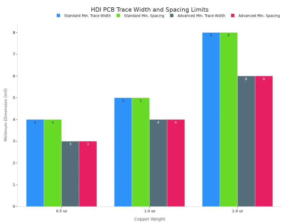
Tight spacing creates crosstalk. Trace spacing below 5 mils amplifies electromagnetic coupling between neighboring traces. Above 1 GHz, that interference degrades performance in telecommunications and data centers. A 12-layer HDI PCB running at 2.5 GHz can show noise up to 10% of the original signal amplitude, which leads to bit errors.
Parameter | Value | Impact on Signal Integrity |
|---|---|---|
Trace spacing in HDI PCBs | Less than 5 mils | Amplifies risk of electromagnetic coupling between neighboring traces |
High frequency threshold | Above 1 GHz | Interference significantly degrades performance in telecommunications and data centers |
Example: 12-layer HDI PCB at 2.5 GHz | Noise up to 10% of original signal amplitude | Leads to bit errors in digital systems, disrupting overall functionality |
The closely spaced traces in HDI designs create a higher probability of inductive and capacitive coupling between lines that causes undesirable voltage spikes, known as crosstalk, leading to data corruption and timing issues with signals.
Maintain at least three times the trace width between high-speed signals. A 4-mil trace should have a 12-mil separation where possible. When space is tight, route high-speed signals on different layers or use differential pairs to cancel noise.
Impedance Control Needs
Impedance-critical traces need sufficient reference plane continuity, with no splits under differential pairs. For high-speed interfaces, prioritize impedance control and stub minimization. Microvias replace long through vias on critical SerDes channels, and simulation-to-measurement correlation becomes a standard release criterion. HDI material selection shifts toward lower-loss dielectrics once data rates exceed 25 Gbps.
Running DFM Checks
Automated DFM Tools
Automated DFM tools check trace widths, spacing, pad sizes, and part placement. Advanced versions automate these checks to reduce respins and cost. They also catch gerber data problems—missing board outlines, wrong drill files, empty or broken data, layer misalignment, and incorrect drill hole sizes—which you must correct before HDI fabrication.
Manual Review of Critical Nets
Automated tools miss context. Review your critical nets by hand. Confirm that differential pair traces stay identical and sit on the same layer. Verify that return paths stay short and loop areas stay small. Check that you did not split ground planes.
Interpreting DFM Reports
Read DFM reports with your fabricator, not alone. Match each check to the manufacturer's capabilities, verify BOM and pick-and-place files against gerber files, and resolve flagged conflicts before release.
DFM check area | What automated DFM tools check | How to interpret HDI DFM reports |
|---|---|---|
Trace width and spacing | Minimum trace/space rules, including same-net spacing that DRC ignores | A fine-pitch breakout at 5/5 mil is at the etch floor; expect effective width 4.2–4.5 mil and adjust impedance/clearance if the report flags marginal width |
Microvia aspect ratio | Laser-drilled microvia depth-to-diameter ratio | 1:1 aspect ratio is standard for laser microvias; deeper features must be mechanically drilled or flagged as manufacturing risk |
Annular ring | Pad diameter vs drill size and drill-wander tolerance | Use pad = drill + 2 × min annular ring + drill tolerance (e.g., 12 mil drill on Class 2 = 18 mil pad); flagged thin rings mean plating breakout risk |
Solder mask dam / fine-pitch BGA | Minimum solder mask dam width and mask expansion | For 0.5 mm pitch BGA, ~8 mil gap leaves 4 mil dam if mask opening equals pad; if report shows no dam after expansion, switch to LDI mask or remove mask between pads |
Component spacing and edge clearance | Distance between parts and board edge | HDI assembly needs 1 mm part spacing (0.5 mm with high precision) and ≥2 mm edge clearance; violations mean pick-and-place/depaneling problems |
Drill aspect ratio | Plated through-hole depth-to-diameter ratio | 8:1 is the practical maximum; higher ratios increase plating-void risk, so a flagged ratio near 10:1 should be redesigned or moved to microvias |
Spotting Gerber File Errors
Layer Alignment Markers
Check that every layer carries alignment markers. Missing or misplaced markers cause layer-to-layer registration errors during lamination.
Drill File Accuracy
Confirm that nc drill files match your fabrication drawings and gerber files. Wrong drill files, incorrect hole sizes, and missing drill data are common gerber file errors that halt production.
Solder Mask Clarity
Verify solder mask openings and dams. Ambiguous mask data leads to exposed copper or bridged pads. Build a short hdi pcb checklist for reviewing gerber data before release: board outline present, drill file matches stackup, mask layers aligned, and all layers share the same origin. This discipline protects manufacturability and prevents costly respins.
How to Resolve HDI Design and Manufacturing Conflicts
You have identified the problem. Now you need a resolution path that satisfies both your performance targets and your fabricator's process limits. The fix rarely comes from one side alone. It comes from structured collaboration, deliberate rule adjustments, and microvia choices that respect production realities.
Early Collaboration with Fabricators
Pre-Layout Design Reviews
Start talking to your fabrication house before you route a single trace. Schedule a design kickoff meeting to review stack-up structures, microvia plans, and component lists. Confirm your design specifications—microvia sizes, trace widths, and spacing—against the manufacturer's equipment limits. If your microvia size exceeds their capability, misalignment or defects will follow. Early confirmation prevents these production issues.
Contact the fabrication house to select materials and obtain dielectric data for creating the PCB stackup. Based on layer count and thickness, determine the via style used to route signals through inner layers. Perform a reliability assessment to verify that materials will not stress interconnects to fracture during assembly or operation. Determine design rules based on fabricator capabilities and reliability requirements, such as tear drops, trace widths, and clearances. Implement the fabricator's DFM and reliability requirements as design rules in your ECAD software on the front end. Stackup creation and design-rule determination are critical to routability, reliability, and manufacturability.
Sharing Stackup Intentions
Request a proposed production stackup from the fabricator before final impedance routing. A late dielectric substitution can alter trace width, spacing, and coupling geometry. Close construction-critical items before final routing: trace width and spacing by layer and copper thickness; laser via diameter, target pad, capture pad, and permitted depth; via-to-copper, via-to-via, and via-to-edge clearances; annular-ring and registration allowances for mechanically drilled holes; via-in-pad filling, planarization, and surface-finish requirements; solder-mask definition around fine-pitch pads; and copper-density balancing expectations.
Avoid combining every published minimum in the same location. Using the smallest trace, spacing, pad, and most complex via structure together makes the board much harder to manufacture. Use the HDI PCB design review checklist as a release gate rather than after-the-fact paperwork. Assign an owner to every open item and withhold production release until construction-critical questions are closed.
Adjusting Design Rules
Relaxing Non-Critical Tolerances
Not every trace needs to be 3 mil. Keep power areas and non-critical routing at relaxed rules—5/5 or 6/6 trace/space—instead of applying 3/3 mil or below board-wide. This avoids over-specification of trace/space, reduces imaging, etching, and registration burden, and improves yield and cost. Simplify the stackup where possible, for example from 2+N+2 to 1+N+1, and separate high-density from low-density routing zones. This lowers lamination cycles, reduces stacked microvia requirements, improves panel yield, and can cut bare-board cost by approximately 15–25%.
Redistributing Routing Density
Consider design redistribution instead of via reduction. Avoid shrinking vias unless routing density actually demands it. This avoids pushing vias into high-aspect-ratio or premium fabrication, improves drill reliability, and lowers cost. Use redistribution layers for congested areas and share vias for non-critical nets. This prevents routing bottlenecks and thermal hotspots, reduces shorts, and avoids costly redesign loops. Compare wiring demand to substrate capacity, then choose the number of routing layers and stack-up accordingly. This ensures enough routing capacity, avoids forcing 1-mil/35-micron trace/space limits, and prevents premium fabrication costs.
Microvia Considerations for Manufacturability
Choosing Reliable Via Structures
Your microvia best practices should start with structure selection. Staggered microvias offset laterally and remove the copper-to-copper interface between successive vias, eliminating a common crack-initiation site. They offer higher field reliability for more than two stacked levels and lower process risk. Stacked microvias align vertically into a continuous copper column, but stress concentrates at each filled junction. They require void-free fill and precise registration at every interface. Skip vias and hybrid structures—microvia plus mechanical through-hole—provide routing flexibility for selective layer connections.
Keep microvia aspect ratios moderate. Ensure thorough desmear after laser drilling. Maintain tight control of plating chemistry. Bake boards to remove moisture. Use symmetric copper distribution to limit warpage. Qualify each production lot against the specific thermal and humidity conditions of the end application, following relevant IPC performance class requirements. Combine in-process inspection, targeted reliability testing, and disciplined process control.
Optimizing Via-in-Pad Processes
Resin-fill and copper-plate vias placed inside pads for fine-pitch BGAs. This stops solder wicking and incomplete joints during reflow. Control blind-via dimple to 25 μm or less to ensure reliable microvia structures and support high-density interconnections. For design features, consider reducing blind via diameter from 0.2 mm to 0.1 mm for laser drilling optimization. Reduce buried via diameter from 0.6 mm to 0.3 mm to improve via-filling manufacturability.
Entrance diameter, taper angle, and residual copper thickness at the via bottom strongly affect subsequent plating quality. Laser energy density and pulse count must be optimized to produce clean via bottoms and residue-free sidewalls. Different dielectric materials respond differently to laser energy, so material-specific process windows are essential.
Match Coefficient of Thermal Expansion (CTE) between PCB substrate and BGA package to prevent warpage, head-in-pillow defects, and cracked solder joints during reflow. Keep pad diameter within ±20–25% of the BGA ball diameter—for example, 0.5 mm ball to 0.4–0.45 mm pad—to avoid insufficient wetting or bridging. Replace complex stacked microvias with staggered microvias or resin-filled through-vias to enable standard processes instead of specialized HDI laser drilling, lowering cost and risk.
Preventing Future HDI Design and Manufacturing Issues
You fixed the immediate defect. Now you must stop it from returning. Prevention separates teams that firefight from teams that ship reliably. Build feedback loops, standardize your DFM guidelines, and invest in training. These three moves turn every failure into a permanent lesson.
Building Feedback Loops
Capturing Manufacturing Data
A feedback loop only works when you capture the right data. Record release-package contents, DFM review findings, and construction notes. Release data includes Gerber files, ODB++ or IPC-2581 output, NC drill files, stackup, via map, and impedance tables. DFM findings cover microvia-to-trace clearance violations, stacked via alignment risks, and copper imbalance. Construction notes document the HDI build-up sequence and microvia spans. Locked process parameters—laser drill energy, lamination pressure, plating current density—establish a fixed baseline. SPC monitoring data such as via diameter distribution and registration accuracy shows drift before it becomes a defect. Batch traceability data lets you trace a field failure back to exact panels and process conditions.
Documenting Root Causes
One HDI project suffered recurring microvia voiding that caused signal-integrity failures. X-ray inspection revealed air pockets inside the vias. Root-cause analysis traced the problem to inconsistent laser drilling that left rough via walls, trapping gases during plating. The team adjusted laser drilling parameters and added a post-drill plasma cleaning step. Voiding dropped significantly, and electrical testing confirmed improved connectivity. Document this kind of analysis so the fix becomes a standard practice, not a one-time repair.
Standardizing DFM Guidelines
Internal Design Rule Checklists
Your internal checklist should anchor to IPC standards. Use IPC-2221 for stack-up symmetry and spacing fundamentals. Apply IPC-2226 for microvia annular ring, via aspect ratio, and registration limits. Reference IPC-6012 Class 3 for plating, via fill, and surface finish criteria. A practical checklist sets minimum 0.025 mm annular ring for laser microvias, laser microvias at 0.075 mm or larger, and VIPPO aspect ratio at 1:1 or below. Derive your rule set from these standards and refresh it when they change.
Aligning with IPC Standards
Review draft rules with your manufacturing partners before layout release. Apply IPC-based inspection protocols during production to verify conductor integrity and registration accuracy. Conduct capability studies before adopting new features such as any-layer vias. This alignment prevents costly redesigns and production delays.
Training and Knowledge Sharing
Design Engineer Fabrication Exposure
Design engineers with hands-on fabrication exposure learn to evaluate real constraints—minimum trace widths, microvia geometry, plating tolerances—before finalizing a layout. This prevents the CAD-perfect design that is difficult to build consistently. Your designers should understand how the board will be fabricated, assembled, and inspected.
Joint Problem-Solving Sessions
Start DFM analysis early with your fabricator and assembly engineer. Validate solder mask clearances against real tolerances. Build and test prototypes before mass production. These sessions catch manufacturability issues before they become misalignments. Apply microvia best practices from every session to your next hdi pcb design.
Advanced Strategies for HDI Conflict Resolution
AI-Driven Analysis
Predictive DFM Models
You can now catch conflicts before fabrication begins. A machine learning model trains on historical layout data combined with real outcomes such as DRC failures, EMI problems, and manufacturing defects. The model then recognizes patterns that frequently cause issues and flags them at an early stage. This goes beyond conventional rule-based DRC. AI introduces a risk layer that catches patterns which satisfy basic rules but tend to fail later, including tight neck-downs, long coupled trace runs, and via patterns that generate stubs.
AI-assisted DFM and DFA checks evaluate whether a board can be reliably built and assembled. The system learns from manufacturing and assembly feedback to warn about defect-prone patterns. It also guides choices like trace widths, via types, and stackups that respect factory limits. A closed-loop learning cycle—design, build, capture issues, and feed results back into AI-driven design rules—continuously strengthens the system's ability to flag design and manufacturing conflicts before fabrication. AI-driven design tools enable real-time manufacturability prediction, allowing recurring production risks such as solder bridging, microvia reliability issues, copper imbalance, and warpage tendencies to be identified during layout development rather than only in post-layout DFM checks. This continuous feedback lets you align early with IPC-2221 design intent and the fabrication capability requirements defined in IPC-6012.
Automated Conflict Flagging
Automated flagging still needs human judgment. A few traces were flagged as possible impedance deviations when inspected in 2D by the CAM team, even though the stackup had already accounted for them, because power pours weren't used as reference returns for the impedance-controlled traces. The original NXP evaluation board hit the same flag on an earlier test run.
This raises the question of whether ODB++ and IPC-2581 formats need richer impedance-profile data so a fab's CAM DFM tools can resolve such flags automatically instead of raising them by hand.
Rapid Prototyping
Short-Run Builds
Rapid PCB prototyping accelerates the production of prototype boards so that electrical performance, mechanical fit, manufacturability, and design assumptions can be validated early in the product lifecycle. Because prototypes can be delivered in days rather than weeks, your team can make faster design decisions and refinements. This early hardware exposure helps reveal signal integrity problems, placement constraints, thermal behavior, and DFM issues before they become expensive. Rapid prototyping also de-risks pilot runs by proving stack-ups, verifying impedance targets, and testing firmware and hardware together.
Electrical and Thermal Testing
Short-run HDI PCB builds surface electrical and thermal issues early. A wearable health device team used two-day prototype PCBs to validate sensor placement and power integrity. An automotive supplier refined ADAS radar front-end designs on controlled impedance boards and reduced signal integrity debug cycles. A telecom OEM achieved first-pass success on 28 Gbps HDI designs using microvias and back-drilling. These examples show how short-run builds support design validation for your most demanding hdi pcb designs.
Supplier Scorecards
Tracking Fabricator Capability
A supplier scorecard turns vague trust into measurable data. Track your fabricator's yield by feature type, microvia reliability, registration accuracy, and on-time delivery. Score each metric against your hdi design requirements. This reveals which suppliers can handle aggressive microvias and which cannot.
Joint Roadmapping
Share your scorecard data with your fabricator. Plan capability upgrades together. Joint roadmapping aligns your next-generation hdi needs with their process investments. This partnership prevents future conflicts before they start.
Key HDI Design and Manufacturing Takeaways
Bridging the Design-Manufacturing Divide
You now hold a complete playbook for how to identify and fix hdi pcb design versus manufacturing issues. The dual approach works because it attacks the problem from both ends. Audits, DFM checks, and Gerber reviews expose the fault. Collaboration, rule adjustments, and microvia choices resolve it. Neither half succeeds alone.
The PCB West 2026 presentation by Stephen V. Chavez on DfM for ultra-high-density interconnects confirms this. It identifies designer-manufacturer collaboration as essential for managing high wiring density, material compatibility, and thermal management. Early integration of DfM principles, industry standardization, and interdisciplinary collaboration make UHDI designs manufacturable, cost-efficient, and scalable. You should confirm process capabilities with your fabricator—such as 25μm trace/space and 0.1mm vias—and use AOI or AXI inspection to catch line width deviations or via voids. Standardized documentation in IPC-2581 format, including drill tables, impedance specs, and BOMs, reduces communication errors. Impedance test correlation keeps theoretical versus physical impedance deviation below 10%.
Building Prevention into Every Project
Prevention is cheaper than correction. This principle should guide every hdi design decision you make. The evidence is clear when you compare the two approaches side by side.
Approach | Cost Impact | Schedule Impact |
|---|---|---|
Prevention (early manufacturer collaboration, DFM checks, simulation, AI analysis, prototyping, feedback loops) | Reduces mistakes, saves money, lowers respins, avoids expensive errors by catching issues early | Keeps projects on schedule; smoother transition from design to production |
Correction (fixing design-manufacturing conflicts after the fact) | Higher costs from extra testing, making new boards, and wasted materials | Delays due to longer inspection and design changes; missed deadlines and late projects |
The conflict between HDI design and manufacturing can hurt your production process. If your design does not fit what the manufacturer can do, you might see delays, more defects like via cracking and open circuits, lower yield, higher costs, and missed deadlines.
You prevent these outcomes through specific actions. Collaborate closely with the manufacturing team and communicate clearly. Use automated DFM tools to check trace widths, spacing, pad sizes, and part placement before sending files. Apply simulation and AI-driven analysis to catch signal, thermal, and manufacturability issues early. Build quick-turn prototypes to find layout, signal, or soldering problems before mass production. Establish feedback loops between design and manufacturing teams, track ECOs and TQs, and run quality control tests like AOI, X-ray, and thermal cycling.
The Competitive Advantage of Alignment
As HDI density increases, design-manufacturing alignment becomes a competitive advantage. Your ability to bridge this divide determines whether you ship reliably or firefight constantly. The hdi pcbs you build tomorrow will demand tighter tolerances, smaller microvias, and more complex stackups. Fabricators who partner with you on joint roadmapping will handle those demands. Suppliers who receive only last-minute files will not.
Treat every project as a chance to strengthen that partnership. Share your stackup intentions early. Document root causes. Standardize your DFM guidelines against IPC standards. Train your designers on fabrication realities. These habits compound over time. They turn manufacturability from a late-stage worry into a front-end design input. That shift gives you speed, yield, and cost advantages your competitors cannot match.
You now have a repeatable path to identify and fix hdi pcb design versus manufacturing issues. Start with systematic audits, DFM checks, and Gerber reviews. Then resolve conflicts through fabricator collaboration and rule adjustments. This dual approach attacks both ends.
Prevention costs far less than correction. Build feedback loops that capture manufacturing data. Standardize your hdi design guidelines against IPC standards. Involve suppliers early. These habits stop defects from returning.
As HDI density climbs, design and manufacturing alignment becomes a competitive advantage. Digital twin technology will reward hdi teams that test virtually before fabrication. Your manufacturability improves when both sides plan together. That partnership delivers lasting speed and yield advantages.
FAQ
How can you tell a design flaw from a manufacturing defect?
Inspect under magnification for plating voids or misregistration. Run electrical tests to reveal opens, shorts, or impedance drift. Use automated optical inspection to flag solder mask damage. Each method exposes a different fault class, so you can name the problem before assigning blame.
Why did my HDI design pass DRC yet fail at the fabricator?
DRC checks your layout rules only. It ignores manufacturing realities like pressed dielectric thickness, registration tolerance, and laser drill limits. A microvia can pass design rule checks yet exceed the fabricator's actual aspect ratio capability. Always audit against real process constraints before release.
What is the maximum microvia aspect ratio you should design for?
Keep laser-drilled microvia aspect ratio at 0.8:1 or lower for standard production. A 0.1 mm diameter via reaches about 0.08 mm maximum reliable depth. Ratios near 1:1 work only on tightly controlled lines and reduce process margin.
How do you fix crosstalk in tightly spaced HDI routing?
Maintain at least three times the trace width between high-speed signals. A 4-mil trace needs 12-mil separation where possible. Alternatively, route high-speed nets on different layers or use differential pairs to cancel coupled noise.
When should you choose stacked rather than staggered microvias?
Use staggered microvias when reliability matters most. They offset laterally, removing the copper-to-copper interface that cracks under stress. Use stacked microvias only when routing density forces vertical alignment, then require void-free fill and precise registration at every junction.
How do you stop solder wicking in via-in-pad designs?
Resin-fill and copper-plate every via placed inside a pad. This stops solder from wicking away during reflow. Control blind-via dimple to 25 μm or less. Unfilled vias produce voids, shorts, and intermittent opens after thermal cycling.
What DFM checks should you run before sending HDI files to fabrication?
Run automated DFM tools to verify trace widths, spacing, pad sizes, and microvia aspect ratios. Review critical nets manually to confirm differential pair symmetry and return paths. Validate Gerber data: board outline, drill files, mask layers, and layer alignment markers all share one origin.
Which standards should govern your HDI design rules?
Anchor your internal design rules to three IPC standards. Use IPC-2221 for stackup symmetry and spacing, IPC-2226 for microvia annular ring and registration limits, and IPC-6012 Class 3 for plating, via fill, and surface finish criteria. Refresh your checklists whenever these standards change.
