IMS PCB Design Considerations for Boards Exceeding 1.5 Meters
Designing an IMS PCB that exceeds 1.5 meters presents a distinct set of engineering challenges. Standard methods often fail to address the scale and complexity involved. Key issues arise in several areas:
Thermal management requires careful material selection and control of dielectric thickness.
Mechanical stability demands strategies to prevent board flexing and manage thermal expansion.
Electrical performance depends on maintaining consistent impedance and signal integrity.
Manufacturing large boards calls for precise drilling and specialized handling.
Industry leaders continue to develop innovative solutions that address these demanding requirements.
Key Takeaways
Large IMS PCBs over 1.5 meters need strong mechanical support to prevent warping and flexing during use and transport.
Effective thermal management uses materials like aluminum alloys and ceramic-filled polymers to spread heat and avoid hotspots.
Maintaining signal integrity and minimizing voltage drop require careful trace design, proper grounding, and power distribution.
Manufacturing large IMS PCBs demands precise handling, thicker boards, and quality control to ensure durability and performance.
Rigorous testing, including Hi-Pot and cycle tests, helps guarantee long-term reliability and prevents insulation or adhesive failures.
Mechanical Stability
Warping Risks
Large-format IMS PCBs face significant risks of warping during both manufacturing and operation. The sheer length of boards exceeding 1.5 meters increases the likelihood of flexing under their own weight. Temperature changes can cause expansion and contraction, which may lead to permanent deformation. Handling and transportation also introduce mechanical stress, especially when the board lacks adequate support. Warping can result in misalignment of components, unreliable connections, and even board failure. Engineers must consider these risks early in the design process to ensure long-term reliability.
Tip: Always assess the installation environment for temperature fluctuations and mechanical loads before finalizing the board design.
Reinforcement Methods
Manufacturers use several strategies to reinforce IMS PCBs and minimize warping. The most common approach involves integrating a metal base layer. This layer, often made from aluminum, copper, or steel, adds rigidity and helps the board maintain its shape. The thickness of the metal base typically ranges from 1 mm to 2 mm, which significantly boosts mechanical strength. Steel-based IMS PCBs provide the highest level of rigidity and resist deformation, making them ideal for harsh environments.
Key industry practices for mechanical reinforcement include:
Using a metal base layer for added rigidity and reduced warping.
Selecting base materials such as aluminum, copper, or steel based on application needs.
Choosing a metal base thickness between 1 mm and 2 mm for optimal strength.
Employing steel bases for maximum durability in demanding conditions.
Leveraging the metal base for both mechanical support and EMI shielding.
Engineers may also add mechanical supports or standoffs along the board’s length. These supports distribute weight evenly and prevent sagging during installation and use. By combining robust material choices with thoughtful mechanical design, manufacturers ensure that large IMS PCBs remain stable and reliable throughout their service life.
IMS PCB Thermal Management
Heat Dissipation
Large IMS PCB designs require advanced thermal management strategies to maintain performance and reliability. Engineers focus on moving heat away from critical components and distributing it evenly across the board. Recent engineering studies highlight several effective techniques for heat dissipation:
Thermal vias, placed under heat-generating components, create direct paths for heat to travel between layers.
Copper pours increase the surface area for heat spreading on both the top and bottom layers.
Strategic component placement separates heat-generating parts from sensitive ones and improves airflow.
Heat sinks attached to high-power components boost the surface area for heat release.
Thermal interface materials, such as pads or pastes, enhance heat transfer between components and heat sinks.
Layout choices, including wider traces, thermal relief connections, and optimized layer stack-ups, help maintain thermal symmetry and support airflow channels.
The metal base layer in IMS PCB designs, usually aluminum, works with a thermally conductive dielectric and copper foil to spread heat quickly and prevent hotspots.
Note: Boards longer than 1.5 meters face unique challenges. Differential thermal expansion between copper and aluminum layers can cause bowing and shear stress in the insulation layer. Thin adhesive insulation layers, while improving heat flow, increase the risk of insulation failure. Engineers must balance these factors with precise control and rigorous testing.
Material Choices
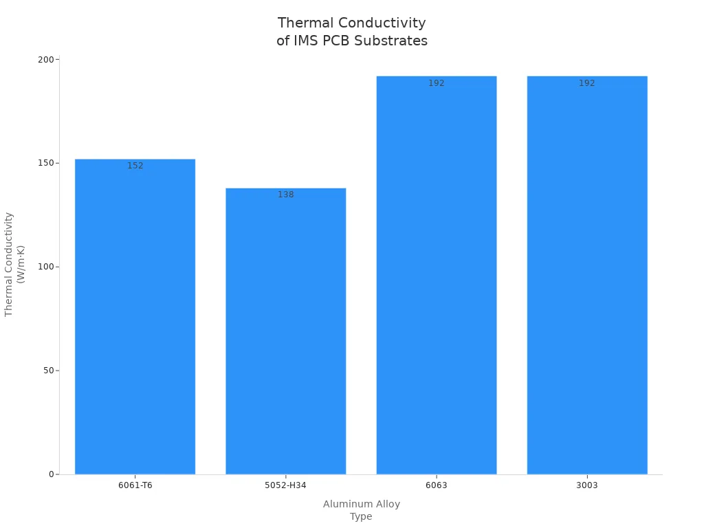
Material selection plays a critical role in the thermal management of IMS PCB assemblies over 1.5 meters. Manufacturers choose substrates and adhesives that offer high thermal conductivity and mechanical stability. Commonly used aluminum alloys include AL5052, AL3003, 6061-T6, 5052-H34, and 6063. These alloys provide thermal conductivity values ranging from approximately 138 to 192 W/m·K, supporting efficient heat dissipation.
Aluminum alloys such as 6061-T6 and 3003 offer high thermal conductivity and are recommended for machining and bending.
The insulation layer between copper and aluminum typically uses a ceramic-filled polymer, which improves both thermal conductivity and mechanical stability.
Ceramic fillers include aluminum oxide, aluminum nitride, boron nitride, magnesium oxide, and silicon oxide.
FR-4 serves as the base PCB material, while surface finishes like HASL, ENIG, and OSP enhance environmental resistance and solderability.
Thicker aluminum substrates (1.5 mm or more) and appropriate copper foil thickness help reduce bowing and improve heat spreading.
Ceramic-filled polymer adhesives outperform traditional glass fiber prepregs in managing thermal flow and mechanical strain.
The following table summarizes how different substrate materials impact thermal conductivity in IMS PCB designs over 1.5 meters:
Substrate Material / Feature | Thermal Conductivity (W/m·K) | Notes |
|---|---|---|
Aluminum Alloy 6061-T6 | 152 | Recommended for machining, good thermal conductivity |
Aluminum Alloy 5052-H34 | 138 | Softer, suitable for bending and punching |
Aluminum Alloy 6063 | 192 | Higher thermal conductivity |
Aluminum Alloy 3003 | 192 | Higher thermal conductivity |
Dielectric Layer Thickness | 0.05 mm – 0.20 mm | Thinner layers improve heat flow but may reduce dielectric strength |
Dielectric Composition | Ceramic-filled polymers | Improves thermal conductivity and reduces strain; fillers include aluminum oxide, aluminum nitride, boron nitride, magnesium oxide, silicon oxide |
Interface Type | Soldered interfaces | 10x - 50x higher thermal conductivity than thermal grease or epoxy |
IMS PCB assemblies with lengths around 1500 mm often use FR-4 combined with aluminum substrates to achieve high thermal conductivity. Surface finishes such as HASL, ENIG, and OSP are standard for enhancing environmental resistance and solderability. These boards serve applications that demand efficient heat dissipation, including horticultural lighting, motor drives, inverters, and solar energy systems. The combination of aluminum alloys, ceramic-filled polymer adhesives, and FR-4 ensures reliable thermal management and mechanical stability.
Tip: Engineers should consider the long-term durability of polymer insulation. Moisture absorption, oxidation, and aging can degrade thermal performance over time. Conservative design derating and rigorous quality control, including Hi-Pot testing, help maintain reliability in large IMS PCB assemblies.
Electrical Performance
Signal Integrity
Signal integrity stands as a critical factor in the design of long-format IMS PCBs. Engineers must address challenges such as signal attenuation, reflections, and electromagnetic interference. Longer traces increase the risk of signal degradation, especially at high frequencies. Consistent impedance throughout the board helps maintain signal quality and prevents reflections that can distort data transmission.
Designers often use controlled impedance traces and differential signaling to preserve signal clarity. Shielding techniques, such as ground planes and metal base layers, reduce electromagnetic interference. Proper trace routing, including minimizing sharp bends and maintaining uniform spacing, supports stable signal transmission. Engineers also conduct signal integrity analysis during the design phase. This analysis identifies potential issues and allows for adjustments before fabrication.
Tip: Place sensitive signal traces away from high-power areas and use simulation tools to predict signal behavior across the entire board length.
Voltage Drop
Voltage drop becomes more pronounced as board length increases. Excessive voltage drop can lead to unstable operation and reduced performance of connected components. Engineers implement several strategies to minimize voltage drop in large IMS PCBs:
Optimize trace width and copper thickness to lower resistance.
Place decoupling capacitors near power pins to stabilize voltage.
Utilize power planes for low-impedance current paths and improved power distribution.
Employ proper grounding techniques, such as star grounding or ground planes, to reduce noise and voltage drop.
Maintain impedance matching to prevent signal reflections and voltage fluctuations.
Conduct voltage drop analysis using advanced simulation tools before fabrication.
Optimize trace routing for efficient current flow.
Implement thermal management strategies, including heat sinks and thermal vias, to prevent heat-related voltage drop effects.
The following table summarizes key design practices for minimizing voltage drop in long-format IMS PCBs:
Design Practice | Benefit |
|---|---|
Wider traces & thicker copper | Lower resistance, reduced voltage drop |
Decoupling capacitors | Stabilized voltage, reduced fluctuations |
Power planes | Improved power distribution |
Proper grounding | Minimized noise and voltage drop |
Simulation tools | Early detection of potential issues |
Engineers who follow these practices ensure reliable electrical performance, even in IMS PCBs exceeding 1.5 meters. Careful planning and analysis help maintain stable operation and extend the lifespan of the board.
Manufacturability with LT CIRCUIT
Production Limits
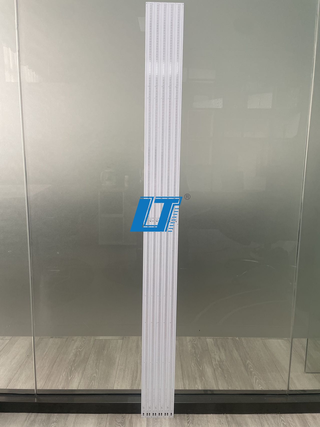
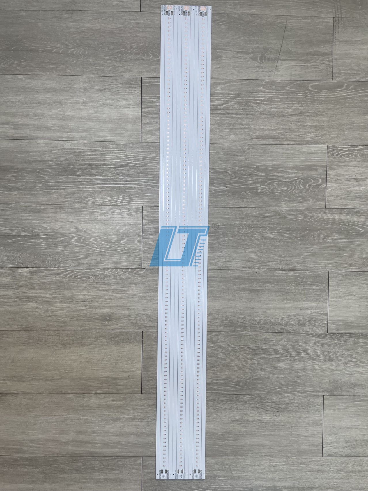
LT CIRCUIT stands out in the electronics manufacturing industry for its ability to produce high-quality IMS PCBs at impressive lengths. The company offers IMS PCBs with a maximum production length of 1200 mm, as demonstrated by their 12-layer IMS PCB product. This length represents the upper limit for IMS PCB manufacturing at LT CIRCUIT, reflecting the brand’s commitment to pushing the boundaries of what is possible in large-format PCB production.
Engineers at LT CIRCUIT use advanced manufacturing processes to ensure precision and reliability, even at these extended lengths. The company’s product range includes HDI PCB boards, multilayer PCB boards, and advanced HDI any layer PCBs. Customers can select from a variety of surface finishes, solder mask colors, and testing services to meet specific project requirements. LT CIRCUIT’s customization options allow for tailored solutions that address unique design and application needs.
Note: LT CIRCUIT holds industry-recognized certifications, including ISO 9001:2015 for quality management, ISO 14001:2015 for environmental responsibility, and ISO 13485:2016 for medical device manufacturing. These certifications demonstrate the company’s dedication to quality, sustainability, and compliance with global standards.
Handling and Assembly
Manufacturing and assembling large IMS PCBs present unique challenges. LT CIRCUIT addresses these challenges with a combination of engineering expertise and strict quality control. The most common handling and assembly issues for boards exceeding 1.5 meters include:
Mechanical stress management during mounting. Precise torque control prevents deformation of the rigid aluminum base and reduces board flexing.
Uniform application of thermal interface material (TIM). A thin, even layer fills microscopic air gaps, ensuring effective heat transfer.
Managing coefficient of thermal expansion (CTE) mismatch. Aluminum expands and contracts more than ceramic components, which can stress solder joints.
Solder joint and underfill adhesive design. Ductile solder alloys, larger solder fillets, and underfill epoxy for BGAs improve reliability.
Avoiding mechanical machining stresses. Placing vias or plated through-holes too close to routed edges can cause deformation or cracking.
Preventing copper pour heat trapping. Large isolated copper areas not connected to the aluminum base can become thermal islands.
Careful board outline design. Avoiding sharp internal corners and narrow necks prevents mechanical weak points.
Panelization, shipping, and handling. Large IMS PCBs require edge protection and weight considerations to prevent damage.
Optimizing thermal via design and layout. Dense arrays of small, filled vias under thermal pads maximize heat dissipation and maintain structural integrity.
LT CIRCUIT uses several strategies to optimize manufacturability for large IMS PCBs:
Thicker PCBs, such as 2.4 mm FR-4, combined with mechanical spacers, prevent sagging and maintain planar stability.
Thicker boards also improve heat dissipation and reduce capacitive effects between signal layers.
PCB-based electrical feedthroughs compatible with vacuum systems reduce cost and complexity.
Python-based interactive design tools enable rapid generation of precise PCB layouts and simulation models, allowing for iterative optimization before fabrication.
Careful design of wiring, connectors, and feedthroughs ensures manufacturability, chemical cleanliness, and organized assembly.
Tip: LT CIRCUIT’s advanced manufacturing capabilities, broad product range, and rigorous quality assurance make it a trusted partner for large-format IMS PCB projects. The company’s certifications validate its ability to deliver reliable, high-performance solutions for demanding applications.
Certification | Description |
|---|---|
ISO 9001:2015 | Quality management and customer satisfaction |
ISO 14001:2015 | Environmental responsibility |
ISO 13485:2016 | Medical device manufacturing standards |
Engineers and project managers can rely on LT CIRCUIT for consistent quality, innovative solutions, and expert support throughout the manufacturing process.
Reliability and Testing
Stress Testing
Engineers rely on rigorous stress testing to ensure IMS PCBs longer than 1.5 meters meet demanding reliability standards. These large boards face unique challenges, including increased risk of bowing, adhesive fatigue, and insulation breakdown. Non-destructive Hi-Pot testing plays a crucial role in verifying dielectric integrity. This test applies a high voltage to the insulation layer, checking for breakdown without causing damage. Cycle testing of the adhesive layer helps assess fatigue performance and detect early signs of delamination, which can compromise thermal flow.
Mechanical stress evaluation focuses on bowing and shear stress caused by differences in thermal expansion between copper and aluminum layers. Larger IMS PCBs often experience higher cumulative strain, making bowing relief and substrate thickness important design factors. High cycle stress testing and accelerated aging protocols simulate years of operation in a condensed timeframe, revealing potential failure points before deployment.
Key reliability metrics for IMS PCBs over 1.5 meters include:
Cycle testing of adhesive layers for fatigue resistance
Hi-Pot testing for insulation integrity
Monitoring for cracking, delamination, and voids
Mechanical stress evaluation for bowing and shear strain
Accelerated aging and high cycle stress testing
LT CIRCUIT’s reliability testing aligns with industry standards such as AEC-Q100 and IPC-9701. Their procedures include pre-test, burn-in, and post-test validation, with temperature ranges tailored to application needs. This approach ensures early detection of defects while maintaining component safety.
Long-Term Performance
Long-term reliability remains a top priority for IMS PCBs in critical applications. Engineers monitor for degradation factors such as polymer aging, water absorption, and oxidation, which can affect insulation properties over time. Non-destructive Hi-Pot testing, performed at voltages above the expected failure threshold, provides a safety margin against insulation breakdown.
Recommended long-term reliability protocols:
Non-destructive Hi-Pot testing for insulation durability
Cycle testing of adhesive layers to prevent delamination
Assessment of adhesive strength above glass transition temperature
Mechanical bowing analysis to protect soldered interfaces
LT CIRCUIT demonstrates a strong commitment to quality and reliability. Their comprehensive testing and quality control processes ensure that large IMS PCBs deliver consistent performance throughout their service life. This dedication has earned LT CIRCUIT industry recognition and trust from customers worldwide.
Tip: For large IMS PCBs, always prioritize conservative design derating and 100% quality control checks to safeguard long-term reliability.
Designers must address several factors when working with IMS PCB assemblies longer than 1.5 meters. Key considerations include mechanical stability, thermal management, electrical performance, and manufacturability. LT CIRCUIT provides advanced solutions and proven expertise for large-format PCB projects.
Engineers can trust LT CIRCUIT for reliable products and comprehensive support.
For more information or to discuss your IMS PCB needs, visit LT CIRCUIT’s official website.
FAQ
What is the maximum length LT CIRCUIT can manufacture for IMS PCBs?
LT CIRCUIT manufactures IMS PCBs up to 1200 mm in length. This capability supports demanding applications that require large-format boards with high reliability and precision.
Which industries use large IMS PCBs from LT CIRCUIT?
Industries such as LED lighting, power electronics, renewable energy, and industrial automation use large IMS PCBs. These sectors require efficient thermal management and robust mechanical stability.
How does LT CIRCUIT ensure quality for long IMS PCBs?
LT CIRCUIT uses advanced testing, including Hi-Pot and cycle tests, and follows strict quality standards like ISO 9001:2015. Engineers monitor every stage to ensure each board meets performance and reliability requirements.
Can LT CIRCUIT customize IMS PCBs for specific project needs?
Yes. LT CIRCUIT offers customization options for layer count, surface finish, solder mask color, and testing services. Customers can request tailored solutions to match their unique application requirements.
See Also
Important Guidelines To Follow When Designing PCB Boards
Typical PCB Design Challenges And Fixes For SMT Technology
Key Advice For Creating Heavy Copper PCBs Handling High Currents